azu_td_1349475_sip1_... - Arizona Campus Repository
azu_td_1349475_sip1_... - Arizona Campus Repository
azu_td_1349475_sip1_... - Arizona Campus Repository
You also want an ePaper? Increase the reach of your titles
YUMPU automatically turns print PDFs into web optimized ePapers that Google loves.
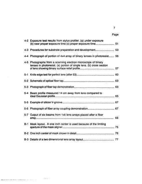
7<br />
Page<br />
4-2 Exposure test results from stylus profiler, (a) under exposure<br />
(b) near proper exposure time (c) proper exposure time 51<br />
4-3 Procedures for substrate preparation and development 53<br />
4-4 Photograph of portion of 4x4 array of binary lenses in photoresist 56<br />
4-5 Photographs from a scanning electron microscope of binary<br />
lenses in photoresist, (a) portion of single lens, (b) cross section<br />
of lens showing binary surface relief profile 57<br />
5-1 Knife edge test for perfect lens (after 53) 60<br />
5-2 Schematic of optical fiber tap 63<br />
5-3 Photograph of fiber tap demonstration 63<br />
5-4 Beam profile measured 14 cm away from lens compared to<br />
ideal Gaussian profile 65<br />
5-5 Example of silicon V-groove 67<br />
5-6 Photograph of fiber array coupling demonstration 67<br />
5-7 Output of six beams from 1 x6 lens arrays placed after a fiber<br />
array 68<br />
B-1 Mask layout. A one inch center is used because of the limiting<br />
aperture of the mask aligner 75<br />
B-2 Oneinchcenterof mask shown in detail 76<br />
B-3 Details of a two dimensional lens array layout 77


