azu_td_1349475_sip1_... - Arizona Campus Repository
azu_td_1349475_sip1_... - Arizona Campus Repository
azu_td_1349475_sip1_... - Arizona Campus Repository
Create successful ePaper yourself
Turn your PDF publications into a flip-book with our unique Google optimized e-Paper software.
45<br />
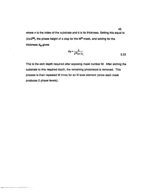
where n is the index of the substrate and d is its thickness. Setting this equal to<br />
(2tc/2 m ), the phase height of a step for the M 111 mask, and solving for the<br />
thickness d M gives<br />
dM = —r^<br />
2<br />
(n* 1 ). 3.23<br />
This is the etch depth required after exposing mask number M. After etching the<br />
substrate to this required depth, the remaining photoresist is removed. This<br />
process is then repeated M times for an N level element (since each mask<br />
produces 2 phase levels).


