FY2010 - Oak Ridge National Laboratory
FY2010 - Oak Ridge National Laboratory
FY2010 - Oak Ridge National Laboratory

Create successful ePaper yourself
Turn your PDF publications into a flip-book with our unique Google optimized e-Paper software.
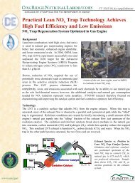
Director’s R&D Fund—<br />
Science for Extreme Environment: Advanced Materials and Interfacial Processes for Energy<br />
Electrical measurements. Impedance spectroscopy was used to study the brush-based metal–insulator–<br />
metal (MIM) structure: heavily doped Si – 2-nm-thick native silicon oxide – ~30-nm-thick PCHD or PPP<br />
brushes. By using a Randles model, our equivalent circuit modeling with undoped PPP brushes suggested<br />
that the contact resistance in the system was 50 times lower than the measured bulk resistance.<br />
The MIM structure without PCHD and PPP brushes had a measured impedance of 1000 ohm and phase of<br />
90 degree over the entire frequency range that we monitored (20–2 million Hz). For the data sets labeled<br />
“air” (i.e., no connection), the low-frequency values are vibrating dramatically, because we are reaching<br />
the higher measuring limit of impedance amplitude at this frequency. The MIM structure with polymer<br />
brushes showed brush-type-dependent impedance behaviors. At 100 Hz, PCHD brushes had AC<br />
impedances that were 20 times higher than those of PPP brushes, while doped PPP brushes showed<br />
10 times lower impedance after 24 h doping in FeCl 3 solution. The doping process was expected to be<br />
slower in brushes than in powder because the dopant could only diffuse from the brush top surface.<br />
Distinctively different AC phase response was also observed upon the PCHD aromatization and PPP<br />
brush formation. The PCHD brush has a phas angle close to 90 degrees, which suggests a nearly pure<br />
capacitor behavior. The corresponding undoped PPP brush has two maxima in the phase-frequency plot:<br />
one at 20 Hz and another at 100,000 Hz, indicating significant resistor-type contributions from interfacial<br />
and orientational polarization mechanisms. The doped PPP brush has an even stronger resistive behavior,<br />
corresponding to a significantly increased R2 and smaller C value in the Randles Circuit as compared to<br />
PCHD and undoped PPP brushes. In addition, we can extrapolate the frequency-dependent impedance to<br />
infinite low frequency in order to estimate DC resistance. The extracted DC conductivity of undoped PPP<br />
brushes were in the range of 10 -10 to 10 -12 S/cm, which is slightly higher than the reported values for<br />
undoped polyacetylene (10 -9 to 10 -10 S/cm).<br />
A microscopic four-point probe (M4PP) was purchased and installed in our Hitachi SEM. It is used either<br />
inside a scanning electron microscopy (SEM) or under an optical microscope to measure DC conductivity<br />
of ultra-thin films. Because we are moving the M4PP into a newly acquired Zeiss SEM, currently we only<br />
managed to use it to measure the conductivity of Nafion/Pt-C composites films on flexible substrates<br />
(Kapton or Teflon). M4PP measurements on a hard substrate such as a silicon wafer or inside the new<br />
Zeiss SEM are still under way.<br />
Patterning. Micropatterning of PPP brushes was successfully achieved with nickel masking and<br />
photolithography. The rough edge shown in the AFM cross-section scan was attributed to the thick nickel<br />
pattern we used (100 nm), which should be easily optimized later on. Currently we are combining e-beam<br />
lithography and nickel masking to make nanopatterns of PPP brushes. A photo-resist pattern generated by<br />
e-beam lithography will be used to pattern PPP brushes.<br />
05195<br />
Controlled Hierarchical Self-Assembly of Robust Organic<br />
Architectures<br />
Benjamin P. Hay, Radu Custelcean, and Nathan C. Duncan<br />
Project Description<br />
The power to predict and control the assembly of matter at the molecular level is the key to unprecedented<br />
control over many intriguing and useful material properties. Although design concepts for the structure-<br />
16