FS2004 Users Manual - FuturePlus Systems
FS2004 Users Manual - FuturePlus Systems
FS2004 Users Manual - FuturePlus Systems

Create successful ePaper yourself
Turn your PDF publications into a flip-book with our unique Google optimized e-Paper software.
simulate a card removal/insertion cycle. The switches are<br />
located on both sides of the termination area To test the<br />
operation of the swap switches, be sure that your PC Card<br />
Software drivers are loaded. Momentarily press both swap<br />
switches simultaneously. Most software drivers will issue a<br />
removal beep followed by an insertion beep. The host socket<br />
controller may remove power when it detects that card detects<br />
have been removed.<br />
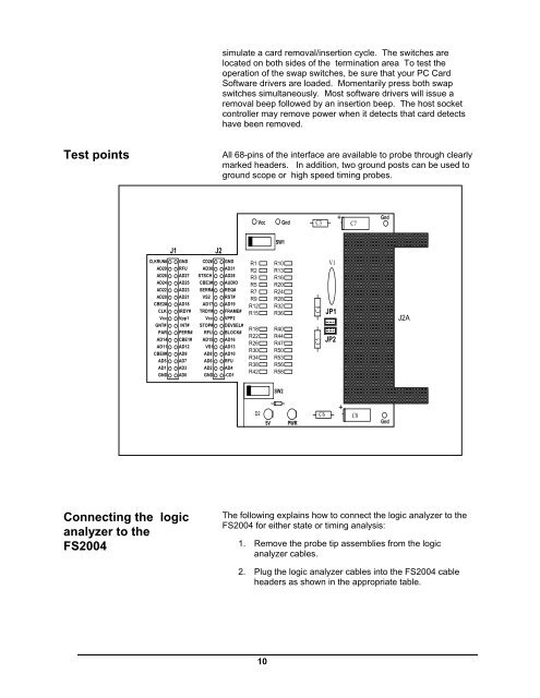
Test points<br />
All 68-pins of the interface are available to probe through clearly<br />
marked headers. In addition, two ground posts can be used to<br />
ground scope or high speed timing probes.<br />
Vcc<br />
Gnd<br />
C3<br />
C7<br />
Gnd<br />
CLKRUN#<br />
AD29<br />
AD26<br />
AD24<br />
AD22<br />
AD20<br />
CBE2#<br />
CLK<br />
Vcc<br />
GNT#<br />
PAR<br />
AD14<br />
AD11<br />
CBE0#<br />
AD5<br />
AD1<br />
GND<br />
J1<br />
GND<br />
RFU<br />
AD27<br />
AD25<br />
AD23<br />
AD21<br />
AD18<br />
IRDY#<br />
Vpp1<br />
INT#<br />
PERR#<br />
CBE1#<br />
AD12<br />
AD9<br />
AD7<br />
AD3<br />
AD0<br />
CD2#<br />
AD30<br />
STSCH<br />
CBE3#<br />
SERR#<br />
VS2<br />
AD17<br />
TRDY#<br />
Vcc<br />
STOP#<br />
RFU<br />
AD15<br />
VS1<br />
AD8<br />
AD6<br />
AD2<br />
GND<br />
J2<br />
GND<br />
AD31<br />
AD28<br />
AUDIO<br />
REQ#<br />
RST#<br />
AD19<br />
FRAME#<br />
VPP2<br />
DEVSEL#<br />
BLOCK#<br />
AD16<br />
AD13<br />
AD10<br />
RFU<br />
AD4<br />
-CD1<br />
R1<br />
R2<br />
R3<br />
R5<br />
R7<br />
R9<br />
R12<br />
R15<br />
R18<br />
R22<br />
R26<br />
R30<br />
R34<br />
R38<br />
R42<br />
SW1<br />
R10<br />
R13<br />
R16<br />
R20<br />
R24<br />
R28<br />
R32<br />
R36<br />
R40<br />
R44<br />
R47<br />
R50<br />
R53<br />
R56<br />
R58<br />
C5 C4<br />
V1<br />
JP1<br />
JP2<br />
J2A<br />
SW2<br />
D2<br />
5V<br />
PWR<br />
C6<br />
C8<br />
Gnd<br />
Connecting the logic<br />
analyzer to the<br />
<strong>FS2004</strong><br />
The following explains how to connect the logic analyzer to the<br />
<strong>FS2004</strong> for either state or timing analysis:<br />
1. Remove the probe tip assemblies from the logic<br />
analyzer cables.<br />
2. Plug the logic analyzer cables into the <strong>FS2004</strong> cable<br />
headers as shown in the appropriate table.<br />
10