You also want an ePaper? Increase the reach of your titles
YUMPU automatically turns print PDFs into web optimized ePapers that Google loves.
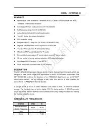
Internet Data Sheet<br />
HY[B/I]18T256[40/80/16]0B[C/F](L)<br />
256-Mbit Double-Data-Rate-Two SDRAM<br />
FIGURE 4<br />
Single-ended AC Input Test Conditions Diagram<br />
<br />
<br />
<br />
<br />
<br />
<br />
<br />
<br />
<br />
<br />
<br />
<br />
<br />
<br />
<br />
<br />
<br />
TABLE 35<br />
Differential DC and AC Input and Output Logic Levels<br />
Symbol Parameter Min. Max. Unit Notes<br />
V IN(dc) DC input signal voltage –0.3 V DDQ + 0.3 —<br />
V ID(dc) DC differential input voltage 0.25 V DDQ + 0.6 —<br />
V ID(ac) AC differential input voltage 0.5 V DDQ + 0.6 V<br />
V IX(ac) AC differential cross point input voltage 0.5 × V DDQ – 0.175 0.5 × V DDQ + 0.175 V<br />
V OX(ac) AC differential cross point output voltage 0.5 × V DDQ – 0.125 0.5 × V DDQ + 0.125 V<br />
1) V IN(dc) specifies the allowable DC execution of each input of differential pair such as CK, CK, DQS, DQS etc.<br />
2) V ID(dc) specifies the input differential voltage V TR – V CP required for switching. The minimum value is equal to V IH(dc) – V IL(dc) .<br />
3) V ID(ac) specifies the input differential voltage V TR – V CP required for switching. The minimum value is equal to V IH(ac) – V IL(ac) .<br />
4) The value of V IX(ac) is expected to equal 0.5 × V DDQ of the transmitting device and V IX(ac) is expected to track variations in V DDQ . V IX(ac)<br />
indicates the voltage at which differential input signals must cross.<br />
5) The value of V OX(ac) is expected to equal 0.5 × V DDQ of the transmitting device and V OX(ac) is expected to track variations in V DDQ . V OX(ac)<br />
indicates the voltage at which differential input signals must cross.<br />
1)<br />
2)<br />
3)<br />
4)<br />
5)<br />
<strong>Rev</strong>. <strong>1.11</strong>, 2007-07 33<br />
11172006-LBIU-F1TN
![Internet Data Sheet HYS72T[32/64]xxxHP-[3S/3.7]-A Rev. 1.01 - UBiio](https://img.yumpu.com/50510224/1/184x260/internet-data-sheet-hys72t32-64xxxhp-3s-37-a-rev-101-ubiio.jpg?quality=85)
![Internet Data Sheet HYB18TC256[80/16]0BF Rev. 1.3 - UBiio](https://img.yumpu.com/50510226/1/184x260/internet-data-sheet-hyb18tc25680-160bf-rev-13-ubiio.jpg?quality=85)


![Internet Data Sheet HY[B/I]39SC128[800/160]FE Rev. 1.1 - UBiio](https://img.yumpu.com/31629373/1/184x260/internet-data-sheet-hyb-i39sc128800-160fe-rev-11-ubiio.jpg?quality=85)