
You also want an ePaper? Increase the reach of your titles
YUMPU automatically turns print PDFs into web optimized ePapers that Google loves.
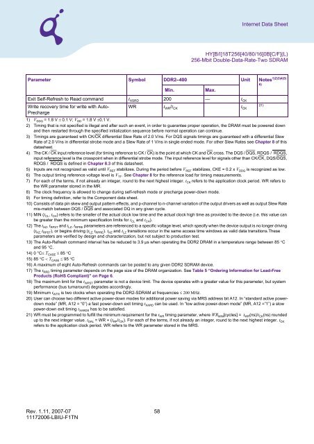
Internet Data Sheet<br />
HY[B/I]18T256[40/80/16]0B[C/F](L)<br />
256-Mbit Double-Data-Rate-Two SDRAM<br />
Parameter Symbol DDR2–400 Unit Notes 1)2)3)4)5)<br />
Exit Self-Refresh to Read command t XSRD 200 — t CK<br />
Write recovery time for write with Auto-<br />
Precharge<br />
WR t WR /t CK t CK<br />
21)<br />
1) V DDQ = 1.8 V ± 0.1 V; V DD = 1.8 V ±0.1 V.<br />
2) Timing that is not specified is illegal and after such an event, in order to guarantee proper operation, the DRAM must be powered down<br />
and then restarted through the specified initialization sequence before normal operation can continue.<br />
3) Timings are guaranteed with CK/CK differential Slew Rate of 2.0 V/ns. For DQS signals timings are guaranteed with a differential Slew<br />
Rate of 2.0 V/ns in differential strobe mode and a Slew Rate of 1 V/ns in single ended mode. For other Slew Rates see Chapter 8 of this<br />
datasheet.<br />
4) The CK / CK input reference level (for timing reference to CK / CK) is the point at which CK and CK cross. The DQS / DQS, RDQS / RDQS,<br />
input reference level is the crosspoint when in differential strobe mode. The input reference level for signals other than CK/CK, DQS/DQS,<br />
RDQS / RDQS is defined in Chapter 8.3 of this datasheet.<br />
5) Inputs are not recognized as valid until V REF stabilizes. During the period before V REF stabilizes, CKE = 0.2 x V DDQ is recognized as low.<br />
6) The output timing reference voltage level is V TT . See Chapter 8 for the reference load for timing measurements.<br />
7) For each of the terms, if not already an integer, round to the next highest integer. t CK refers to the application clock period. WR refers to<br />
the WR parameter stored in the MR.<br />
8) The clock frequency is allowed to change during self-refresh mode or precharge power-down mode.<br />
9) For timing definition, refer to the Component data sheet.<br />
10) Consists of data pin skew and output pattern effects, and p-channel to n-channel variation of the output drivers as well as output Slew Rate<br />
mis-match between DQS / DQS and associated DQ in any given cycle.<br />
11) MIN (t CL , t CH ) refers to the smaller of the actual clock low time and the actual clock high time as provided to the device (i.e. this value can<br />
be greater than the minimum specification limits for t CL and t CH ).<br />
12) The t HZ , t RPST and t LZ , t RPRE parameters are referenced to a specific voltage level, which specify when the device output is no longer driving<br />
(t HZ, t RPST ), or begins driving (t LZ, t RPRE ). t HZ and t LZ transitions occur in the same access time windows as valid data transitions.These<br />
parameters are verified by design and characterization, but not subject to production test.<br />
13) The Auto-Refresh command interval has be reduced to 3.9 µs when operating the DDR2 DRAM in a temperature range between 85 °C<br />
and 95 °C.<br />
14) 0 °C≤ T CASE ≤ 85 °C<br />
15) 85 °C < T CASE ≤ 95 °C<br />
16) A maximum of eight Auto-Refresh commands can be posted to any given DDR2 SDRAM device.<br />
17) The t RRD timing parameter depends on the page size of the DRAM organization. See Table 5 “Ordering Information for Lead-Free<br />
Products (RoHS Compliant)” on Page 6.<br />
18) The maximum limit for the t WPST parameter is not a device limit. The device operates with a greater value for this parameter, but system<br />
performance (bus turnaround) degrades accordingly.<br />
19) Minimum t WTR is two clocks when operating the DDR2-SDRAM at frequencies ≤ 200 ΜΗz.<br />
20) User can choose two different active power-down modes for additional power saving via MRS address bit A12. In “standard active powerdown<br />
mode” (MR, A12 = “0”) a fast power-down exit timing t XARD can be used. In “low active power-down mode” (MR, A12 =”1”) a slow<br />
power-down exit timing t XARDS has to be satisfied.<br />
21) WR must be programmed to fulfill the minimum requirement for the t WR timing parameter, where WR MIN [cycles] = t WR (ns)/t CK (ns) rounded<br />
up to the next integer value. t DAL = WR + (t RP /t CK ). For each of the terms, if not already an integer, round to the next highest integer. t CK<br />
refers to the application clock period. WR refers to the WR parameter stored in the MRS.<br />
Min.<br />
Max.<br />
6)<br />
<strong>Rev</strong>. <strong>1.11</strong>, 2007-07 58<br />
11172006-LBIU-F1TN
![Internet Data Sheet HYS72T[32/64]xxxHP-[3S/3.7]-A Rev. 1.01 - UBiio](https://img.yumpu.com/50510224/1/184x260/internet-data-sheet-hys72t32-64xxxhp-3s-37-a-rev-101-ubiio.jpg?quality=85)
![Internet Data Sheet HYB18TC256[80/16]0BF Rev. 1.3 - UBiio](https://img.yumpu.com/50510226/1/184x260/internet-data-sheet-hyb18tc25680-160bf-rev-13-ubiio.jpg?quality=85)


![Internet Data Sheet HY[B/I]39SC128[800/160]FE Rev. 1.1 - UBiio](https://img.yumpu.com/31629373/1/184x260/internet-data-sheet-hyb-i39sc128800-160fe-rev-11-ubiio.jpg?quality=85)