
Create successful ePaper yourself
Turn your PDF publications into a flip-book with our unique Google optimized e-Paper software.
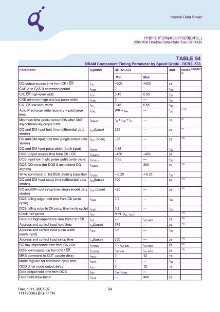
Internet Data Sheet<br />
HY[B/I]18T256[40/80/16]0B[C/F](L)<br />
256-Mbit Double-Data-Rate-Two SDRAM<br />
TABLE 54<br />
DRAM Component Timing Parameter by Speed Grade - DDR2–533<br />
Parameter Symbol DDR2–533 Unit Notes 1)2)3)4)5)<br />
DQ output access time from CK / CK t AC –500 +500 ps<br />
CAS A to CAS B command period t CCD 2 — t CK<br />
CK, CK high-level width t CH 0.45 0.55 t CK<br />
CKE minimum high and low pulse width t CKE 3 — t CK<br />
CK, CK low-level width t CL 0.45 0.55 t CK<br />
Auto-Precharge write recovery + precharge t DAL WR + t RP — t CK<br />
7)17)<br />
time<br />
Minimum time clocks remain ON after CKE t DELAY t IS + t CK + t IH –– ns<br />
8)<br />
asynchronously drops LOW<br />
DQ and DM input hold time (differential data t DH (base) 225 –– ps<br />
9)<br />
strobe)<br />
DQ and DM input hold time (single ended data t DH1 (base) –25 — ps<br />
10)<br />
strobe)<br />
DQ and DM input pulse width (each input) t DIPW 0.35 — t CK<br />
DQS output access time from CK / CK t DQSCK –450 +450 ps<br />
Min.<br />
Max.<br />
6)<br />
DQS input low (high) pulse width (write cycle) t DQSL,H 0.35 — t CK<br />
DQS-DQ skew (for DQS & associated DQ t DQSQ — 300 ps<br />
signals)<br />
10)<br />
Write command to 1st DQS latching transition t DQSS – 0.25 + 0.25 t CK<br />
DQ and DM input setup time (differential data t DS (base) 100 — ps<br />
10)<br />
strobe)<br />
DQ and DM input setup time (single ended data t DS1 (base) –25 — ps<br />
10)<br />
strobe)<br />
DQS falling edge hold time from CK (write t DSH 0.2 — t CK<br />
cycle)<br />
DQS falling edge to CK setup time (write cycle) t DSS 0.2 — t CK<br />
Clock half period t HP MIN. (t CL, t CH )<br />
11)<br />
Data-out high-impedance time from CK / CK t HZ — t AC.MAX ps<br />
12)<br />
Address and control input hold time t IH (base) 375 — ps<br />
10)<br />
Address and control input pulse width t IPW 0.6 — t CK<br />
(each input)<br />
Address and control input setup time t IS (base) 250 — ps<br />
10)<br />
DQ low-impedance time from CK / CK t LZ(DQ) 2 × t AC.MIN t AC.MAX ps<br />
13)<br />
DQS low-impedance from CK / CK t LZ(DQS) t AC.MIN t AC.MAX ps<br />
13)<br />
MRS command to ODT update delay t MOD 0 12 ns<br />
Mode register set command cycle time t MRD 2 — t CK<br />
OCD drive mode output delay t OIT 0 12 ns<br />
Data output hold time from DQS t QH t HP –t QHS —<br />
Data hold skew factor t QHS — 400 ps<br />
<strong>Rev</strong>. <strong>1.11</strong>, 2007-07 54<br />
11172006-LBIU-F1TN
![Internet Data Sheet HYB18TC256[80/16]0BF Rev. 1.3 - UBiio](https://img.yumpu.com/50510226/1/184x260/internet-data-sheet-hyb18tc25680-160bf-rev-13-ubiio.jpg?quality=85)
![Internet Data Sheet HYS72T[32/64]xxxHP-[3S/3.7]-A Rev. 1.01 - UBiio](https://img.yumpu.com/50510224/1/184x260/internet-data-sheet-hys72t32-64xxxhp-3s-37-a-rev-101-ubiio.jpg?quality=85)


![Internet Data Sheet HY[B/I]39SC128[800/160]FE Rev. 1.1 - UBiio](https://img.yumpu.com/31629373/1/184x260/internet-data-sheet-hyb-i39sc128800-160fe-rev-11-ubiio.jpg?quality=85)