

Advanced CAD System for Electromagnetic MEMS Interactive Analysis
Advanced CAD System for Electromagnetic MEMS Interactive Analysis
Advanced CAD System for Electromagnetic MEMS Interactive Analysis

You also want an ePaper? Increase the reach of your titles
YUMPU automatically turns print PDFs into web optimized ePapers that Google loves.
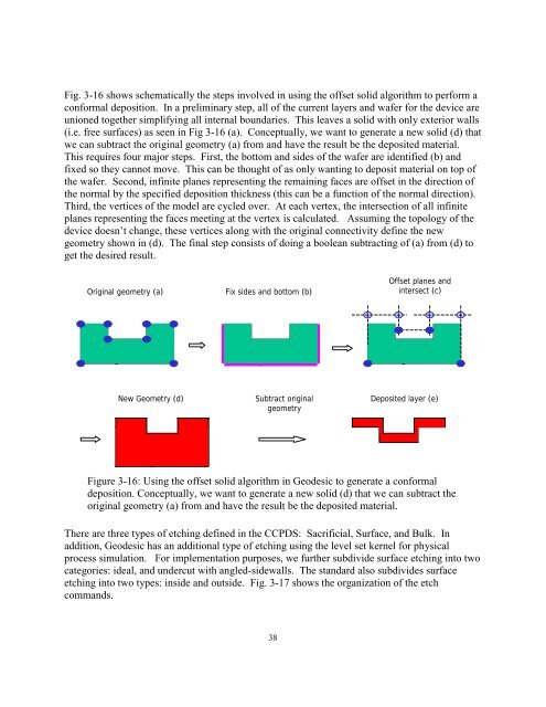
Fig. 3-16 shows schematically the steps involved in using the offset solid algorithm to per<strong>for</strong>m a<br />
con<strong>for</strong>mal deposition. In a preliminary step, all of the current layers and wafer <strong>for</strong> the device are<br />
unioned together simplifying all internal boundaries. This leaves a solid with only exterior walls<br />
(i.e. free surfaces) as seen in Fig 3-16 (a). Conceptually, we want to generate a new solid (d) that<br />
we can subtract the original geometry (a) from and have the result be the deposited material.<br />
This requires four major steps. First, the bottom and sides of the wafer are identified (b) and<br />
fixed so they cannot move. This can be thought of as only wanting to deposit material on top of<br />
the wafer. Second, infinite planes representing the remaining faces are offset in the direction of<br />
the normal by the specified deposition thickness (this can be a function of the normal direction).<br />
Third, the vertices of the model are cycled over. At each vertex, the intersection of all infinite<br />
planes representing the faces meeting at the vertex is calculated. Assuming the topology of the<br />
device doesn’t change, these vertices along with the original connectivity define the new<br />
geometry shown in (d). The final step consists of doing a boolean subtracting of (a) from (d) to<br />
get the desired result.<br />
Original geometry (a)<br />
New Geometry (d)<br />
Fix sides and bottom (b)<br />
Subtract original<br />
geometry<br />
Figure 3-16: Using the offset solid algorithm in Geodesic to generate a con<strong>for</strong>mal<br />
deposition. Conceptually, we want to generate a new solid (d) that we can subtract the<br />
original geometry (a) from and have the result be the deposited material.<br />
There are three types of etching defined in the CCPDS: Sacrificial, Surface, and Bulk. In<br />
addition, Geodesic has an additional type of etching using the level set kernel <strong>for</strong> physical<br />
process simulation. For implementation purposes, we further subdivide surface etching into two<br />
categories: ideal, and undercut with angled-sidewalls. The standard also subdivides surface<br />
etching into two types: inside and outside. Fig. 3-17 shows the organization of the etch<br />
commands.<br />
38<br />
Offset planes and<br />
intersect (c)<br />
Deposited layer (e)


