Advanced CAD System for Electromagnetic MEMS Interactive Analysis
Advanced CAD System for Electromagnetic MEMS Interactive Analysis
Advanced CAD System for Electromagnetic MEMS Interactive Analysis
Create successful ePaper yourself
Turn your PDF publications into a flip-book with our unique Google optimized e-Paper software.
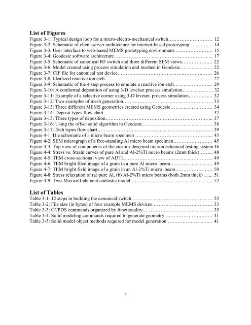
List of Figures<br />
Figure 3-1: Typical design loop <strong>for</strong> a micro-electro-mechanical switch……………………… 12<br />
Figure 3-2: Schematic of client-server architecture <strong>for</strong> internet-based prototyping……….….. 14<br />
Figure 3-3: User interface to web-based <strong>MEMS</strong> prototyping environment…………………... 15<br />
Figure 3-4: Geodesic software architecture………………………………………………….... 17<br />
Figure 3-5: Schematic of canonical RF switch and three different SEM views………………. 22<br />
Figure 3-6: Model created using process simulation and meshed in Geodesic…………….…. 22<br />
Figure 3-7: CIF file <strong>for</strong> canonical test device…………………………………………….…… 26<br />
Figure 3-8: Idealized reactive ion etch………………………………………………………... 27<br />
Figure 3-9: Schematic of the 4 step process to emulate a reactive ion etch…………………... 29<br />
Figure 3-10: A con<strong>for</strong>mal deposition of using 3-D levelset process simulation………….…… 32<br />
Figure 3-11: Example of a selective corner using 3-D leveset. process simulation…………... 32<br />
Figure 3-12: Two examples of mesh generation………………………………………………. 33<br />
Figure 3-13: Three different <strong>MEMS</strong> geometries created using Geodesic…………………….. 34<br />
Figure 3-14: Deposit types flow chart…………………………………………………………. 37<br />
Figure 3-15: Three types of deposition………………………………………………………... 37<br />
Figure 3-16: Using the offset solid algorithm in Geodesic……………………………………. 38<br />
Figure 3-17: Etch types flow chart…………………………………………………………….. 39<br />
Figure 4-1: Die schematic of a micro beam specimen ………………………………………... 45<br />
Figure 4-2: SEM micrograph of a free-standing Al micro beam specimen…………………… 45<br />
Figure 4-3: Top view of components of the custom-designed micromechanical testing system 46<br />
Figure 4-4: Stress vs. Strain curves of pure Al and Al-2%Ti micro beams (2mm thick)……... 48<br />
Figure 4-5: TEM cross-sectional view of Al3Ti………………………………………………. 49<br />
Figure 4-6: TEM bright filed image of a grain in a pure Al micro beam…………………….. 49<br />
Figure 4-7: TEM bright field image of a grain in an Al-2%Ti micro beam………………….. 50<br />
Figure 4-8: Stress relaxation of (a) pure Al, (b) Al-2%Ti micro beams (both 2mm thick) …... 51<br />
Figure 4-9: Two-Maxwell-element anelastic model ………………………………………….. 52<br />
List of Tables<br />
Table 3-1: 12 steps in building the canonical switch …………………………………….…… 23<br />
Table 3-2: File size (in bytes) of four example <strong>MEMS</strong> devices………………………………. 33<br />
Table 3-3: CCPDS commands organized by functionality……………………………….…… 35<br />
Table 3-4: Solid modeling commands required to generate geometry ………………….……. 41<br />
Table 3-5: Solid model object methods required <strong>for</strong> model generation ……………….……... 41<br />
v


