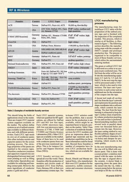
RF & WirelessTable 2: Examples of worldwide foundry servicesThis should bring the fields ofapplications closer to the reader.There are 4 main LTCC materialsystem suppliers available onthe market. The authors definesystems as set of unfired ceramictape available in different thicknessand with different permittivities.Each LTCC tape needsits own set of conductor pastes(this often includes resistor andcapacitor pastes) for the screenprinting process. The shrinkageproperties of the pastes arematched to the ceramic tapes.There fore conductors (resistorsand capacitors respectively) aredistinguished between inner andouter printing as well as fillingvia thru-holes. Special alloys areavailable for soldering and bondingcontact pads. However, themain ingredients of conductorpastes is gold and silver.Such LTCC material systems,which are qualified for RF applications,are offered by DuPont(951 and 943: low loss tape),Ferro (A6M: microwave tape,A6S: low cost microwave tape),Heraeus (CT700, CT800 andCT2000) and Electro-ScienceLaboratories (ESL). Other LTCCtapes are available on the market.Some of them have to be usedwith conductor pastes from oneof the previous mentioned suppliers.This is for instance CeramTecand Nippon ElectricalGlass (NEG).LTCC foundry services arespread all over the world. Thesefoundries offer the production ofmodules and circuits made ofstandard LTCC from DuPont,Ferro, Hereaus, ESL or their ownsupplementary ceramic tape. Thein-house LTCC solution couldrise the problem, that a secondsource for the production is notavailable, which might be animportant factor to launch a producton the market. Table 2 listsa selection of worldwide foundryservices for LTCC modules andgives an impression about theapplied tape materials and theproduction capabilities (as far asthese information could be foundout). Beyond these foundries anumber of companies have itsown LTCC production facilities,which are not available forcustomers.Bosch, Hitachi and Murata aretypical firms, who manufacturetheir own LTCC products for theautomotive, mobile communicationand consumer electronicmarkets.LTCC manufacturingprocessThe manufacturing steps formultilayer LTCC starts with thepreparation of the unfired ceramictape and is finished withthe inspection of the completedmodule. This process, which issimilar at all facilities, is illustratedin figure 1. The followingsection describes the manufacturingsteps with the example ofIMST’s sample and prototypeproduction line. The process isorganized to be compatible tomost of those foundry services,which utilize the unconstrainedsintering method.The green or unfired LTCC foilis delivered on a roller or as couponsin pre-confected sizes. Thefoil from the roller will be cut tofit into the manufacturing equipment(3.5 inch by 3.5 inch forIMST). In the next step the tapewill be processed under a YAGlaser,which is also used to trimresistors. The laser cuts 4 positionholes in each corner and anadditional one for the orientationof the coupon into the tape.A layout tool reads all cavitiesand vias from the layer’s artworkand implements the position andshape coordinates into a softwarecode, which controls the lasercutting. The dust from the laserburning is exhausted to keep thetape’s surface clean of particles.In volume production punchingof vias and cavities is preferred.Special punching machines withseveral tools in parallel shootsome ten thousand holes perminute into the tape. However,the laser cutting method is veryflexible (arbitrary shapes of cavitiesand different diameters forvia holes) and cheaper for prototyping,which results in thesame quality.In the next manufacturing stepthe vias will be filled with conductorpaste. This is done witha screen printer: a stainless steelstencil with the same via holeslike the tape is aligned abovethe ceramic. A doctor blade issqueezing down the paste thruthe stencil into the via, while avacuum pump below the porousnest helps to fill the via with the68 hf-praxis 9/<strong>2015</strong>
RF & Wirelessconductor ink. This techniqueenables the fabrication of solidfilled via connections from onelayer to an other. Typical diametersare 250 μm, 150 μm butalso 100 μm are possible, whichis a requirement for RF applications.In the next step the screenprinter is used to print the conductorpastes and also the resistoror capacitor pastes onto theceramic foil. In standard screenprint technology a line resolutionof 100 μm (line width and spacing)is achievable. It has beendemonstrated that 30 μm is possiblewith a special screen printerand a standard conductor paste.Other techniques are availableto enhance the line resolution:photoimageable pastes for innerand outer conductors (e.g. Fodelfrom DuPont or TC2301PI fromHeraeus), etched conductors orthinfilm on LTCC (post-fired, ontop or button only).An optical inspection followedthe processing of each singleLTCC layer. This way faultylayers can be identified earlyand can be sorted out. All perfectcoupons will be stackednext. The simplest way to proceedis to stack each tape on atool with adjust pins for the positionholes. In volume productionspecial stacking machines carryout this job with an accuracy ofa few micrometer. The LTCClayers have to be laminated inthe next step. Two techniquesare used in practice: the uniaxialpressing which is often used inproduction as well as the isostaticpressing.The first method is like coiningmoney, where the LTCC stackis pressed between two parallelplates, which are heated up.A drawback here is, that largertolerances in the substratethickness will appear afterfiring, because the plates arenear a hundred percent in parallel.Another difficulty is theuniaxial pressing with cavitiesin the LTCC stack. The cavitywill be deformed due to the fact,that the strong pressure operatesonto the edges only. The alternativemethod is the isostaticlamination. The tool uses waterheated up to 80 °C as a medium1. Unconstrained or Free Sintering:: 2. Constrained Sintering or Zero-ShrinkageX-, Y-shrinkage ≈ 13 % ± 0.3 % X-, Y-shrinkage ≈ 0.1 % ± 0.05 %Z-shrinkage ≈ 15 % ± 0.5 % Z-shrinkage ≈ 45 % ± 0.4 %Table 3: Two co-firing methodsto uniformly distribute the forceof the lamination. A pressure of300 psi is recommended. Thisprocess minimizes the de-laminationand gives more uniformshrinkage, which improves theyield of complex parts. Layersto be laminated are stacked ona backing plate before they aresealed in a flexible vacuum bag.Inserts may be used as an optionto ensure accurate cavities. Theseare the reasons, why IMST decidedto install an isostatic laminatorfor its prototyping process.The sintering of the stack ina process furnace follows thelamination procedure. A specifictemperature-time profile,which depends on the glass-ceramicmixture, has to be observedduring the firing process. LTCCsuppliers deliver such profileswithin their design rules. Atypical practice is to heat up theoven to 450 °C with a gradient ofabout 2 - 5 °C per minute. Theorganic solvents have to escapecompletely during this period. Inthe next 30 minutes the temperatureis raised to about 880 °C,where the sintering process ofthe glass starts. This temperatureremains constant for nearly15 minutes to finish the sintering.A controlled cooling of thefurnace to room-temperature isperformed in the last phase ofthe firing process, which takesat least 3 hours. Table 3 showstwo co-firing methods are usedin practice.The zero-shrinkage process usestwo additional tape layers whichhave to be co-laminated to thepackage of the unfired LTCCtapes. These two layers constrainthe shrinking of the LTCCduring the firing. The constrainingtapes do not shrink or sinteritself, but maintain a uniformlyhigh frictional contact to the surfaceof the LTCC. With the helpof this method it is possible toreduce shrinking to about 0.05%to 0.15% with a tolerance of0.05% depending on the design.This process has its advantage inmanufacturing large tiles 6 inchx 6 inch). However, the volumeproduction of modules withcavities is not yet established.That was the reason for IMSTto decide for a free sinteringprocess, where cavities for RFmodules can easily be fabricated.The sintered LTCC substratesare now ready for inspection andpost-processing. Typical stepsare further screen prints of conductorsor resistors, which is alsocalled post-firing, the dicing ofcircuits from the wafer and theassembly processes like wirebonding or SMD technology.IMST has accredited measurementlaboratories to characterizecircuits up to 110 GHz andantennas up to 60 GHz as wellas an EMC-qualification centerto perform relevant tests for theCE sign.LMDS-Module as anApplication ExampleLMDS stands for local multipointdistribution services,where digital radio networksare applied to local regions likeurban and company areas orothers. Central multipoint basestations (relay stations) supplyterminals with data in a wirelessnetwork. Services like localcomputer networks, digital voiceand video as well as others areoffered. There are several frequencybands allocated fromEuropean organizations likeCEPT (European Conferenceof Postal and TelecommunicationsAdministrations) or ERO(European Radio CommunicationOffice). Recommendationsregulate the use and specificationsof these band. The onefor the 24.5 GHz to 26.5 GHzband is called “T/R 13-02”.Corresponding to this standarda transceiver module has beendesigned, fabricated, assembledand evaluated. Figure 2 shows aphoto of the circuit.Ferro’s A6M LTCC tape withgold conductors on the top andsilver conductors for inner layershave been used. 5 substratelayers are required for microstripand stripline waveguides withinthe module. Monolithic integratedGaAs-circuits (MMICs) aremounted into simple and steppedcavities to obtain optimaltransitions from the Chips to theLTCC environment.In figure 2 the position of theMMICs is illustrated: attenuator(Att), amplifier (Amp), mixer,low noise amplifier (LNA) andpower amplifier (PA). Bandpassfilters (BP), Wilkinson powerdivider and tripler are realizedin LTCC to keep the module’scosts low. DC supply lines arecrossing over the bandpass filters,which are completely buriedas L-shaped stripline segments.The module consists of threebranches: the transmit, receiveand local oscillator path. Doublerows of via chains are shieldingthe branches within the LTCCsubstrates. Metal walls in thecap are connected with these viafences for an optimal shielding.SMA connectors are utilizedfor the IF and LO ports, whileGPO connectors from Gilbertare used for the RF ports. Allthis results in a very compactand cost effective transceivermodule for LMDS applications.The size of the LTCC substratewithin the Aluminium housingis 30 x 55 mm.Further InformationBooklet:“LTCC - An Introduction andOverview”, IMST GmbH,December 2001http://www.ltcc.deltcc@imst.dehf-praxis 9/<strong>2015</strong> 69