10-2020
Fachzeitschrift für Hochfrequenz- und Mikrowellentechnik
Fachzeitschrift für Hochfrequenz- und Mikrowellentechnik

Erfolgreiche ePaper selbst erstellen
Machen Sie aus Ihren PDF Publikationen ein blätterbares Flipbook mit unserer einzigartigen Google optimierten e-Paper Software.
APPLICATION SPOTLIGHT<br />
RF PCB Design: AWR with Allegro<br />
Designers face multiple challenges when incorporating RF/microwave, analog, and digital design elements together on<br />
the same PCB. These multi-layer PCBs, which are commonly used in next-generation commercial and military applications,<br />
are densely populated with high-speed data lines and RF circuitry and are prone to coupling/crosstalk and other<br />
parasitic behavior that can impair system performance.<br />
To successfully integrate RF/microwave content and mixed-signal designs, PCB layout tools and RF circuit design<br />
software must exchange design data efficiently. AWR software offers an RF/microwave intellectual property (IP) creation<br />
platform with import and export functionality to provide a pathway to and from Cadence Allegro or OrCAD ® PCB design<br />
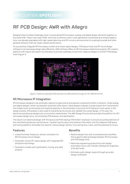
tools (Figure 1).<br />
Figure 1: Cadence originated PCB imported into AWR software through an IPC-2581 file format<br />
RF/Microwave IP Integration<br />
RF/microwave designers use schematic capture to place active and passive components within a network. Unlike analog<br />
and digital designs, which use parasitic extraction after layout, these designs typically include closed-form transmission<br />
line models (such as microstrip and stripline) explicitly in the schematic to account for RF behavior much earlier in the<br />
design process. EM analysis is also used to characterize structures and validate the overall design. In this way, the<br />
electrical and physical designs are concurrently implemented. The AWR Design Environment provides the platform for RF/<br />
microwave design entry, circuit/system/EM analysis, and optimization.<br />
The result is an electrical design with the layout and PCB stackup information necessary to ensure accurate prediction of<br />
the manufactured device’s performance. Transferring this layout and stackup information into the Cadence PCB layout<br />
and routing platform eliminates the need for manual design reentry, thus saving time, costs, and the potential for errors.<br />
Features<br />
f<br />
f<br />
f<br />
Linear/nonlinear frequency-domain simulation for<br />
RF/microwave circuit design<br />
Schematic-driven RF-aware design with integrated EM<br />
extraction technology<br />
Parametric studies with optimization, tuning, and yield<br />
analysis<br />
Benefits<br />
f<br />
f<br />
f<br />
Reduce design time with a comprehensive workflow<br />
that supports data exchange between RF/microwave<br />
and PCB design tools<br />
Maximize engineering productivity with design<br />
automation and a user-friendly interface for engineers<br />
of all skill levels<br />
Eliminate costly design respins through accurate<br />
design verification<br />
www.cadence.com/go/awr<br />
1