mitac 8355.pdf - tim.id.au
mitac 8355.pdf - tim.id.au
mitac 8355.pdf - tim.id.au
You also want an ePaper? Increase the reach of your titles
YUMPU automatically turns print PDFs into web optimized ePapers that Google loves.
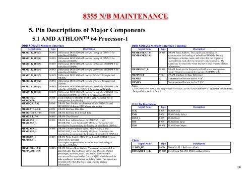
DDR SDRAM Memory Interface<br />
Signal Name Type Description<br />
MEMCLK_H/L[7] O-IOD Differential DDR SDRAM clock to the top of DIMM 0 for<br />
unbuffered DIMMs. 1<br />
MEMCLK_H/L[6] O-IOD Differential DDR SDRAM clock to the top of DIMM 0 for<br />
unbuffered DIMMs. 1<br />
MEMCLK_H/L[5] O-IOD Differential DDR SDRAM clock to the bottom of DIMM 0 for<br />
unbuffered DIMMs. 1<br />
MEMCLK_H/L[4] O-IOD Differential DDR SDRAM clock to the bottom of DIMM 0 for<br />
unbuffered DIMMs. 1<br />
MEMCLK_H/L[3] O-IOD Differential DDR SDRAM clock to DIMM 3 for registered<br />
DIMMs. 1<br />
MEMCLK_H/L[2] O-IOD Differential DDR SDRAM clock to DIMM 3 for registered<br />
DIMMs. 1<br />
MEMCLK_H/L[1] O-IOD Differential DDR SDRAM clock to the m<strong>id</strong>dle of DIMM 1 for<br />
unbuffered DIMMs, or DIMM 1 for registered DIMMs. 1<br />
MEMCLK_H/L[0] O-IOD Differential DDR SDRAM clock to the m<strong>id</strong>dle of DIMM 1 for<br />
unbuffered DIMMs, or DIMM 1 for registered DIMMs. 1<br />
MEMCKEA<br />
O-IOS Clock Enables to DIMMs. Used to gate clocks for power<br />
MEMCKEB<br />
management functionality. 1<br />
MEMDQS[17:0] B-IOS DRAM Data Strobes synchronous with MEMDATA and<br />
MEMCHECK during DRAM read and writes. 1<br />
MEMDATA[63:0] B-IOS DRAM Interface Data Bus<br />
MEMCHECK[7:0] B-IOS DRAM Interface ECC Check Bits<br />
MEMCS_L[7:0] O-IOS DRAM Chip Selects 1<br />
MEMRASA_L<br />
MEMRASB_L<br />
MEMCASA_L<br />
MEMCASB_L<br />
MEMWEA_L<br />
MEMWEB_L<br />
MEMADDA[13:0]<br />
MEMADDB[13:0]<br />
O-IOS<br />
O-IOS<br />
O-IOS<br />
O-IOS<br />
8355 N/B MAINTENANCE<br />
5. Pin Descriptions of Major Components<br />
5.1 AMD ATHLON TM 64 Processor-1<br />
DRAM Row Address Select. MEMRASA_L and<br />
MEMRASB_L are functionally <strong>id</strong>entical. Two copies are<br />
prov<strong>id</strong>ed to accommodate the loading of unbuffered DIMMs. 1<br />
DRAM Column Address Select. MEMCASA_L and<br />
MEMCASB_L are functionally <strong>id</strong>entical. Two copies are<br />
prov<strong>id</strong>ed to accommodate the loading of unbuffered DIMMs.1<br />
DRAM Write Enable. MEMWEA_L and MEMWEB_L are<br />
functionally <strong>id</strong>entical.<br />
Two copies are prov<strong>id</strong>ed to accommodate the loading of<br />
unbuffered DIMMs. 1<br />
DRAM Column/Row Address. Two copies are prov<strong>id</strong>ed to<br />
accommodate the loading of unbuffered DIMMs. During<br />
precharges, activates, reads, and writes, the two copies<br />
are inverted from each other (except A[10] which is used for<br />
<strong>au</strong>to-precharge) to minimize switching noise. The signals are<br />
inverted only when the bus is used to carry address<br />
information. 1<br />
DDR SDRAM Memory Interface Continue<br />
Signal Name Type Description<br />
MEMBANKA[1:0]<br />
MEMBANKB[1:0]<br />
O-IOS<br />
DRAM Bank Address. Two copies are prov<strong>id</strong>ed to<br />
accommodate the loading of unbuffered DIMMs. During<br />
precharges, activates, reads, and writes the two copies are<br />
inverted from each other to minimize switching noise. The<br />
signals are inverted only when the bus is used to carry address<br />
information. 1<br />
MEMRESET_L O-IOS DRAM Reset pin for Suspend-to-RAM power management<br />
mode. This pin is required for registered DIMMs only.<br />
MEMVREF VREF DRAM Interface Voltage Reference 1<br />
MEMZP A Compensation Resistor tied to VSS 1<br />
MEMZN A Compensation Resistor tied to 2.5 V 1<br />
Notes:<br />
1. For connection details and proper resistor values, see the AMD Athlon 64 Processor Motherboard<br />
Design Gu<strong>id</strong>e, order# 24665.<br />
JTAG Pin Descriptions<br />
Signal Name Type Description<br />
TCK I-IOS JTAG Clock<br />
TMS I-IOS JTAG Mode Select<br />
TRST_L I-IOS JTAG Reset<br />
TDI I-IOS JTAG Data Input<br />
TDO O-IOS JTAG Data Output<br />
Clock<br />
Signal Name Type Description<br />
CLKIN_H/L I-IOD 200-MHz PLL Reference Clock<br />
FBCLKOUT_H/L O-IOD Core Clock PLL 200-MHz Feedback Clock<br />
100


