mitac 8355.pdf - tim.id.au
mitac 8355.pdf - tim.id.au
mitac 8355.pdf - tim.id.au

You also want an ePaper? Increase the reach of your titles
YUMPU automatically turns print PDFs into web optimized ePapers that Google loves.
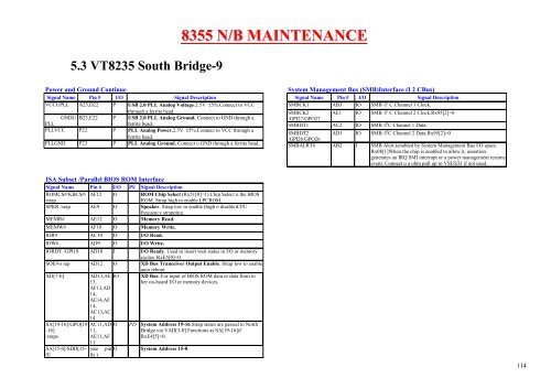
5.3 VT8235 South Br<strong>id</strong>ge-9<br />
Power and Ground Continue<br />
Signal Name Pin # I/O Signal Description<br />
VCCUPLL A23,D22 P USB 2.0 PLL Analog Voltage.2.5V ±5%.Connect to VCC<br />
through a ferrite bead.<br />
GNDU B23,E22 P USB 2.0 PLL Analog Ground. Connect to GND through a<br />
PLL<br />
ferrite bead.<br />
PLLVCC P22 P PLL Analog Power.2.5V ±5%.Connect to VCC through a<br />
ferrite bead.<br />
PLLGND P23 P PLL Analog Ground. Connect o GND through a ferrite bead.<br />
ISA Subset /Parallel BIOS ROM Interface<br />
Signal Name Pin # I/O PU Signal Description<br />
ROMCS#/KBCS#/ AF12 O ROM Chip Select (Rx51[0]=1).Chip Select o the BIOS<br />
strap<br />
ROM. Strap high to enable LPCROM.<br />
SPKR /srap AE9 O Speaker. Strap low to enable (high o disable)CPU<br />
frequency strapping.<br />
MEMR# AE12 O Memory Read.<br />
MEMW# AF10 O Memory Write.<br />
IOR# AC10 O I/O Read.<br />
IOW# AD9 O I/O Write.<br />
IORDY /GPI19 AD10 I I/O Ready. Used to insert wait states in I/O or memory<br />
cycles. RxE5[0]=0<br />
SOE#/s rap AD12 O XD Bus Tranceiver Output Enable. Strap low to enable<br />
<strong>au</strong>to reboot.<br />
XD[7-0] AD13,AE IO XD Bus. For input of BIOS ROM data or data from to<br />
13,<br />
AF13,AD<br />
14,<br />
AE14,AF<br />
14,<br />
AC13,AC<br />
14<br />
her on-board I/O or memory devices.<br />
SA[19-16]/GPO[19 AC11,AD O PD System Address 19-16.Strap states are passed to North<br />
-16]<br />
11,<br />
Br<strong>id</strong>ge via VAD[3-0].Functions as SA[19-16]if<br />
/sraps<br />
AE11,AF<br />
11<br />
RxE4[5]=0.<br />
SA[15-0]/SDD[15- (see pin O System Address 15-0.<br />
0]<br />
lis )<br />
8355 N/B MAINTENANCE<br />
System Management Bus (SMB)Interface (I 2 CBus)<br />
Signal Name Pin # I/O Signal Description<br />
SMBCK1 AB3 IO SMB /I 2 C Channel 1 Clock.<br />
SMBCK2<br />
/GPI27/GPO27<br />
AE1 IO SMB /I 2 C Channel 2 Clock.Rx95[2]=0<br />
SMBDT1 AC2 IO SMB /I 2 C Channel 1 Data.<br />
SMBDT2<br />
/GPI26/GPO26<br />
AD1 IO SMB /I 3 C Channel 2 Data.Rx95[2]=0<br />
SMBALRT# AB2 I SMB Alert.(enabled by System Management Bus I/O space<br />
Rx08[1]When the chip is enabled to allow it, assertion<br />
generates an IRQ SMI interrupt or a power management resume<br />
event. Connect o a ohm pull up to VSUS33 if not used.<br />
114