mitac 8355.pdf - tim.id.au
mitac 8355.pdf - tim.id.au
mitac 8355.pdf - tim.id.au

Create successful ePaper yourself
Turn your PDF publications into a flip-book with our unique Google optimized e-Paper software.
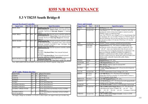
5.3 VT8235 South Br<strong>id</strong>ge-8<br />
Internal Keyboard Controller<br />
Signal Name Pin # I/O PU Signal Description<br />
MSCK /IRQ1 W2 IO/I PU MultiFunction Pin (Internal mouse controller enabled by<br />
Rx51[1]) Rx51[1]=1 Mouse Clock. From internal mouse<br />
controller. Rx51[1]=0 Interrupt Request 1 .Interrupt<br />
input 1.<br />
MSDT /IRQ12 W1 IO/I PU MultiFunction Pin (Internal mouse controller enabled by<br />
Rx51[1]) Rx51[1]=1 Mouse Data. From internal mouse<br />
controller. Rx51[1]=0 Interrupt Request 12. Interrupt<br />
input 12.<br />
KBCK /KA20G V3 IO /I PU MultiFunction Pin (Internal keyboard controller enabled<br />
by Rx51[0]) Rx51[0]=1 Keyboard Clock. From internal<br />
keyboard controller Rx51[0]=0 Gate A20.Input from<br />
external keyboard controller.<br />
KBDT /KBRC V2 IO/I PU MultiFunction Pin (Internal keyboard controller enabled<br />
by<br />
Rx51[0])<br />
Rx51[0]=1 Keyboard Data. From internal keyboard<br />
controller.<br />
Rx51[0]=0 Keyboard Reset. From external keyboard<br />
controller (KBC)for CPURST# generation<br />
KBCS#/ROMCS#/srap AF12 O/O Keyboard Chip Select (Rx51[0]=0).To external<br />
keyboard controller chip. Strap high o enable LPC ROM:<br />
Note: KBCK,KBDT,MSCK,and MSDT are powered by the VSUS33 suspend voltage plane.<br />
AC97 Audio /Modem Interface<br />
Signal Name Pin # I/O Signal Description<br />
ACRST# R3 O AC97 Reset.<br />
ACBTCK T3 I AC97 Bit Clock.<br />
ACSYNC T1 O AC97 Sync.<br />
ACSDO U1 O AC97 Serial Data Out.<br />
ACSDIN0 (VSUS33) T2 I AC97 Serial Data In 0.<br />
ACSDIN1 (VSUS33) U3 I AC97 Serial Data In 1.<br />
ACSDIN2 /GPIO20 /PCS0# U2 I AC97 Serial Data In2.RxE4[6]=0,E5[1]=0,PMIO<br />
Rx4C[20]=1<br />
ACSDIN3/GPIO21<br />
V1 I AC97 Serial Data In 3.RxE4[6]=0,E5[2]=0,PMIO<br />
/PCS1#/SLPBTN#<br />
Rx4C[21]=1<br />
The supply voltage for ACSDIN0-1 is VSUS33 so these inputs can support wake-up on modem ring<br />
8355 N/B MAINTENANCE<br />
Power and Ground<br />
Signal Name Pin # I/O Signal Description<br />
VCC33 (see pin list)v P I/O Power.3.3V ±5%<br />
VCC (see pin list) P Core Power.2.5V ±5%.This supply is turned on only when he<br />
mechanical switch on the power supply is turned on and he<br />
PWRON signal is conditioned high .<br />
Note: The VT8235L core voltage is 2.5V so board designs that<br />
are intended t all w use of either VT8235 or VT8235L should<br />
take this difference into account and allow the core voltage to<br />
be selected as either 2.5V (for the VT8235)or 3.3V (for the<br />
VT8235L).<br />
GND (see pin list) P Ground. Connect o primary motherboard ground plane.<br />
VSUS33 AA4,AB4,<br />
AC4,AC5<br />
P Suspend Power.3.3V ±5%.Always available unless the<br />
mechanical switch of the power supply is turned off. If the<br />
“soft-off”state is not implemented, then this pin can be<br />
Connected to VCC33.Signals powered by or referenced o this<br />
plane are:PWRGD, RSMRST#,PWRBTN#,SMBCK1/2,<br />
SMBDT1/2,GPO0,SUSA#/GPO1,SUSB#/ GPO2,SUSC#,<br />
SUSST1#/GPO3,SUSCLK /GPO4,GPI1,GPI2/EXTSMI#,GPI3<br />
/RING#,GPI4 /LID,GPI5 /BATLOW#,GPI6 /PME#,<br />
SMBALRT#<br />
VSUS25 T4,U4 P Suspend Power.2.5V ±5%.<br />
VSUSUSB D15 P USB Suspend Power.2.5V ±5%.<br />
VBAT AE4 P RTC Battery. Battery input for internal RTC<br />
(RTCX1,RTCX2)<br />
VLVREF J23 P V-Link Voltage Reference.0.9V ±5%.0.34 xVCC25to0.38<br />
xVCC25.<br />
VCCVK (see pin list) P V-Link Compensation Circuit Voltage.2.5V ±5%<br />
MIIVCC D11,D12,<br />
E11,E12<br />
P LAN MII Power.3.3V ±5%.Power for LAN Media<br />
Independent Interface (interface to external PHY).Connect o<br />
VCC33 through a ferrite bead.<br />
MIIVCC25 D13,E13 P LAN MII Suspend Power.2.5V ±5%.<br />
RAMVCC E7 P LAN RAM Power.2.5V ±5%.Power for LAN internal RAM.<br />
Connect to VCC through a ferrite bead.<br />
RAMGND E8 P LAN RAM Ground. Connect o GND through a ferrite bead.<br />
USBVCC (see pin list) P USB 2.0 Differential Output Power.3.3V ±5%.Power for<br />
USB differential outputs (USBP0+,P0 –,P1+,P1 –,P2+,<br />
P2 –, P3+, P3 –,P4+,P4 –,P5+,P5 –).Connect o VSUS33<br />
through a ferrite bead.<br />
USBGND (see pin list) P USB 2.0 Differential Output Ground. Connect to GND<br />
through a ferrite bead.<br />
113