mitac 8355.pdf - tim.id.au
mitac 8355.pdf - tim.id.au
mitac 8355.pdf - tim.id.au

You also want an ePaper? Increase the reach of your titles
YUMPU automatically turns print PDFs into web optimized ePapers that Google loves.
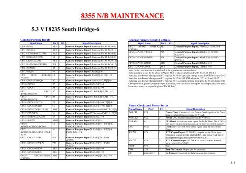
5.3 VT8235 South Br<strong>id</strong>ge-6<br />
General Purpose Inputs<br />
Signal Name Pin # I/O Signal Description<br />
GPI0 (VBAT) AE3 I General Purpose Input 0.Status on PMIO Rx20[0]<br />
GPI1 (VSUS33) AC3 I General Purpose Input 1.Status on PMIO Rx20[1]<br />
GPI2 /EXTSMI#(VSUS33) AA1 I General Purpose Input 2.Status on PMIO Rx20[4]<br />
GPI3 /RING#(VSUS33) Y2 I General Purpose Input 3.Status on PMIO Rx20[8]<br />
GPI4 /LID#(VSUS33) AC1 I General Purpose Input 4.Status on PMIO Rx20[11]<br />
GPI5 /BATLOW#(VSUS33) W4 I General Purpose Input 5.Status on PMIO Rx20[12]<br />
GPI6 /AGPBZ# A8 I General Purpose Input 6.Status on PMIO Rx20[5]<br />
GPI7 /REQ5# N4 I General Purpose Input 7.RxE4[2]=0<br />
GPI8 /GPO8 /PDREQA C8 I General Purpose Input8. RxE4[3]=0, E5[4]=0,<br />
/VGATE<br />
53[7]=0<br />
GPI9 /GPO9 /PDREQB B7 I General Purpose Input 9. RxE4[3]=0,53[7]=0<br />
GPI10 /GPO10 D7 I General Purpose Input 10.RxE4[3]=0<br />
GPI11 /GPO11 A6 I General Purpose Input 11.RxE4[3]=0<br />
GPI12 /GPO12 A7 I General Purpose Input 12. RxE4[4]=0,5B[1]=0,<br />
/INTE#/PDGNTA<br />
53[7]=0<br />
GPI13 /GPO13 B8 I General Purpose Input 13. RxE4[4]=0,5B[1]=0,<br />
/INTF#/PDGNTB<br />
53[7]=0<br />
GPI14 /GPO14 /INTG# D8 I General Purpose Input 14.RxE4[4]=0,5B[1]=0<br />
GPI15 /GPO15/INTH# C7 I General Purpose Input 15.RxE4[4]=0,5B[1]=0<br />
GPI16 /INTRUDER#(VBAT) AD3 I General Purpose Input 16.Status on PMIO Rx20[6]<br />
GPI17 /CPUMISS Y1 I General Purpose Input 17.Status on PMIO Rx20[5]<br />
GPI18 /THRM#/AOLGPI Y4 I General Purpose Input 18.Rx8C[3]=0<br />
GPI19 /IORDY AD10 I General Purpose Input 19.RxE5[0]=1<br />
GPI20<br />
U2 I General Purpose Input 20.RxE4[6]=1,E5[1]=0,<br />
/GPO20/ACSDIN2/PCS0#<br />
PMIO 4C[20]=1<br />
GPI21<br />
V1 I General Purpose Input 21.RxE4[6]=1,E5[2]=0<br />
/GPO21/ACSDIN3/PCS1#/SLP<br />
BTN#<br />
PMIO 4C[21]=1<br />
GPI22 /GPO22 /GHI# R24 I General Purpose Input 22.RxE5[3]=1,PMIO<br />
4C[22]=1<br />
GPI23 /GPO23 /DPSLP# P26 I General Purpose Input 23.RxE5[3]=1,PMIO<br />
4C[23]=1<br />
GPI24 /GPO24/GPIOA AE5 I General Purpose Input 24.RxE6[0]=0<br />
GPI25 /GPO25/GPIOC AE6 I General Purpose Input 25.RxE6[1]=0<br />
GPI26 /GPO26/SMBDT2<br />
(VSUS33)<br />
8355 N/B MAINTENANCE<br />
AD1 I General Purpose Input 26.Rx95[2]=1,95[3]=0<br />
General Purpose Inputs Continue<br />
Signal Name Pin # I/O Signal Description<br />
GPI27 /GPO27 /SMBCK2 AE1 I General Purpose Input 27.Rx95[2]=1,95[3]=0<br />
(VSUS33)<br />
GPI28 /GPO28 /VIDSEL P25 I General Purpose Input 28.RxE5[3]=1,PMIO<br />
4C[28]=1<br />
GPI29 /GPO29/VRDSLP P24 I General Purpose Input 29.RxE5[3]=1,PMIO<br />
4C[29]=1<br />
GPI30 /GPO30 /GPIOD AD6 I General Purpose Input 30.RxE6[6]=0<br />
GPI31 /GPO31/GPIOE AC6 I General Purpose Input 31.RxE6[7]=0<br />
Note:Def<strong>au</strong>l pin function is underlined in he signal name column above.<br />
Note:Input pin s a us for he above GPI pins 31-0 is also available on PMIO Rx4B-48 [31-0 ]<br />
Note:See also Power Management I/O register Rx50 for input pin change status for GPI16-19 and 24-27<br />
Note:See also Power Management I/O register Rx52 for SCI/SMI select for GPI16-19 and 24-27<br />
Note:See also Power Management I/O register Rx4C.General purpose input pins 20-31 are shared with<br />
OD (open drain)general purpose output functions,so to use one of these pins as an input pin,a one must<br />
be written to the corresponding bit of PMIO Rx4C.<br />
Resets,Clocks,and Power Status<br />
Signal Name Pin # I/O Signal Description<br />
PWRGD AF4 I Power Good. Connected o he Power Good signal on he Power<br />
Supply. Internal logic powered by VBAT.<br />
PWROK# AE2 O Power OK. Internal logic powered by VSUS33.<br />
PCIRST# R2 O PCI Reset. Active low reset signal for he PCI bus. The VT8235<br />
will assert his pin during power-up or from he control register.<br />
OSC AC12 I Oscillator.14.31818 MHz clock signal used by he in ernal<br />
Timer.<br />
RTCX1 AD4 I RTC Crystal Input :32.768 KHz crystal or oscilla or input.<br />
This input is used for the internal RTC and power-well power<br />
management logic and is powered by VBAT.<br />
RTCX2 AF3 O RTC Crystal Output :32.768 KHz crystal output. Internal<br />
logic powered by VBAT.<br />
TEST AF9 I Test.<br />
TPO U24 O Test Pin Output. Output pin for est mode.<br />
NC W22,AD17 - No Connect. Reserved for future use,do not connect.<br />
111