mitac 8355.pdf - tim.id.au
mitac 8355.pdf - tim.id.au
mitac 8355.pdf - tim.id.au

Create successful ePaper yourself
Turn your PDF publications into a flip-book with our unique Google optimized e-Paper software.
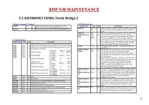
“Hyper Transport” Control<br />
HTRST# B11 O Hyper Transport Reset.Connect to RESET# pin of K8<br />
CPU.2.5V swing.Active when the RESET# input is active<br />
HTSTP# A12 I Hyper Transport Stop. Connect to South Br<strong>id</strong>ge DPSLP# pin<br />
V-Link Interface<br />
Signal Name Type I/O Description<br />
VAD7,<br />
VAD6<br />
VAD5<br />
VAD4<br />
VAD3<br />
VAD2<br />
VAD1,<br />
VAD0<br />
AF25<br />
AD24<br />
AF20<br />
AE19<br />
AE24<br />
AF24<br />
AD21<br />
AD20<br />
VPAR AF19 IO Parity<br />
VBE# AE21 IO Byte Enable<br />
8355 N/B MAINTENANCE<br />
5.2 K8T800M(VT8385) North Br<strong>id</strong>ge-2<br />
Address/Data Bus.Also used to pass strap information from the south<br />
IO br<strong>id</strong>ge to the north br<strong>id</strong>ge (the physical strap is not on the north br<strong>id</strong>ge<br />
IO VAD pin of the south br<strong>id</strong>ge with the information passed over to the<br />
IO north br<strong>id</strong>ge at reset <strong>tim</strong>e)<br />
IO<br />
Connection Register SB Pin<br />
IO VAD7-Test Mode L=Disable, n/a SDCS3#<br />
IO<br />
H=Enable<br />
IO VAD6-ROMSIP L=Disable, Rx51[7] SDA2<br />
IO<br />
H=Enable<br />
VAD5-Loop Test Mode L=Disable, n/a SDA1<br />
H=Enable<br />
VAD4-reserved n/a n/a SAD0<br />
VAD3-Fast Command L=Disable, Rx53[7] SA19<br />
H=Enable<br />
VAD2-HT Bus W<strong>id</strong>th L=8 bits, n/a SA18<br />
H=16 bits<br />
VAD1-HT Bus Frequency Msb LL=200MHz RxCC[9] SA17<br />
LH=400MHz<br />
VAD0-HT Bus Frequency Lsb LL=600MHz RxCC[8] SA16<br />
LH=800MHz<br />
UPCMD AF26 I Command from Client(South Br<strong>id</strong>ge) to Host(North Br<strong>id</strong>ge)<br />
UPSTB AE23 I Strobe from Client to Host<br />
UPSTB# AF23 I Complement Strobe form Client to Host<br />
DNCMD AD23 O Command from Host(North Br<strong>id</strong>ge) to Client(South Br<strong>id</strong>ge)<br />
DNSTB AF22 O Strobe from Host to Client<br />
DNSTB# AD22 O Complement Strobe form Host to Client<br />
AGP Bus Interface<br />
Signal Name Type I/O Description<br />
GD[31:0] (See pin<br />
list<br />
GBE[3:0]<br />
(GBE[3:0#] for 4x<br />
mode<br />
AC7<br />
AD11<br />
AF11<br />
AD11<br />
IO Address / Data Bus. Address is deiven with GDS assertion for<br />
AGP-style transfers and with GFRM# assertion for PCI-stle<br />
IO<br />
trafers.<br />
Command /byte Enable (interpreted as C/BE# for AGP 2x/4x<br />
And (C# /BE# for PCI ) driven by the master (graphics<br />
controller) when requests are being enqueued using GPIPE#<br />
2x/4x only as GPIPE# isn’t used in 8x mode). These pin<br />
prov<strong>id</strong>e val<strong>id</strong>e byte information during AGP write transaction<br />
And are driven by master. Thfe target (this chip) drives these<br />
line to “0000” during the return of AGP read data. For PCI<br />
cycles, commands are driven on gollowing clocks<br />
GPAR AC16 IO AGP Parity A single parity bit is prov<strong>id</strong>ed over GD[31:0]<br />
and GBE[3:0]..<br />
GDBIH /GPIPE# AC5 IO Dynamic Bus inversion High /Low. AGP 8x transfer mode<br />
GDBIL<br />
AC4 only. Driven by the source to indicate whether the<br />
corresponding data bit group should be inverted). Used to<br />
limit thenamber of simultaneously switching outputs to 8 for<br />
each 16-pin group.<br />
Pipelined Request. Not used by AGP 8x. Asserted by the<br />
master external graphics the master enqueues one request is to<br />
be enqueued by the target (North br<strong>id</strong>ge ) The master<br />
enqueues one request each rising edge of GCLK while<br />
GPIPE# is asserted. When GPIPE# is deasserted no new<br />
requests are enqueued across the AD bus<br />
Note: See RxAE[1] for GPIPE# GDBIH pin function selection<br />
GDS0F (GDS0 for AE15 IO Bus Strobe 0. Source synchronous strobes for GD[15:0] (the<br />
4x)<br />
agent that is prov<strong>id</strong>ing the data drives these signals) GDS0<br />
GDS0S (GDS0# for AF15 prov<strong>id</strong>es <strong>tim</strong>ing for 2x data transfer mode: GDS0 and GDS0#<br />
4x)<br />
Prov<strong>id</strong>e <strong>tim</strong>ing for 4x mode. For 8x transfer mode, GDS0 is<br />
interpreted as GDS0F (“First strobe) and GDS0# as<br />
GDS0S(“second” strobe )<br />
GDS1F (GDS1 for AE7 IO Bus Strobe 1. Source synchronous strobes for GD[31:16] (i.<br />
4x)<br />
e , the agent that is prov<strong>id</strong>ing the data drives these signals ).<br />
GDS1S GDS1# for AF7 GDS1 prov<strong>id</strong>es <strong>tim</strong>ing for 2x data transfer mode: GDS1 and<br />
4x)<br />
GDS1F (“first” strobe) and GDS1# as GDSIS (“second”<br />
strobe)<br />
GFRM (GFRM# for AC9 IO Frame. Assertion indicates the address phase of a PCI/ transfer<br />
4x)<br />
. Negation indicates that one more date transfer is desired by<br />
the cycle initiator interpreted as active high for AGP 8x.<br />
103