mitac 8355.pdf - tim.id.au
mitac 8355.pdf - tim.id.au
mitac 8355.pdf - tim.id.au

Create successful ePaper yourself
Turn your PDF publications into a flip-book with our unique Google optimized e-Paper software.
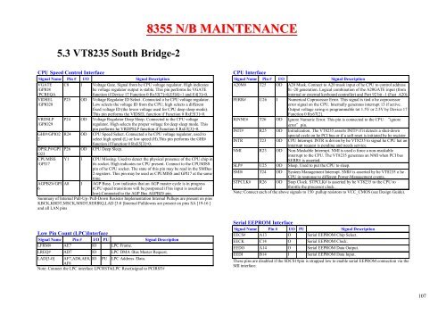
5.3 VT8235 South Br<strong>id</strong>ge-2<br />
CPU Speed Control Interface<br />
Signal Name Pin # I/O Signal Description<br />
VGATE C8 I Voltage Gate. Signal from he CPU voltage regulator. High indicates<br />
/GPIO8<br />
he voltage regulator output is stable. This pin performs he VGATE<br />
/PCREQA<br />
function if Device 17 Function 0 Rx53[7]=0,E5[4]=1 and E4[3]=0.<br />
VIDSEL P25 OD Voltage Regulator ID Select. Connected o he CPU voltage regulator.<br />
/GPIO28<br />
Low selects the voltage ID from the CPU; high selects a different<br />
fixed voltage ID (the lower voltage used for CPU deep sleep mode).<br />
This pin performs the VIDSEL function if Function 0 RxE5[3]=0.<br />
VRDSLP P24 OD Voltage Regulator Deep Sleep. Connected to the CPU voltage<br />
/GPIO29<br />
regulator. High selects the proper voltage for deep sleep mode. This<br />
pin performs he VRDPSLP function if Function 0 RxE5[3]=0.<br />
GHI#/GPIO2 R24 OD CPU Speed Select. Connected o he CPU voltage regulator, used to<br />
2<br />
select high speed (L) or low speed (H).This pin performs the GHI#<br />
function if Function 0 RxE5[3]=0.<br />
DPSLP#/GPI<br />
O23<br />
P26 OD CPU Deep Sleep.<br />
CPUMISS Y1 I CPU Missing. Used to detect the physical presence of the CPU chip in<br />
/GPI17<br />
its socket. High indicates no CPU present. Connect to the CPUMISS<br />
pin of he CPU socket. The state of this pin may be read in the SMBus<br />
2 registers. This pin may be used as CPUMISS and GPI17 at the same<br />
<strong>tim</strong>e.<br />
AGPBZ#/GPI A8 I AGP Busy. Low indicates that an AGP master cycle is in progress<br />
6<br />
(CPU speed transitions will be postponed if his input is asserted<br />
low).Connected to the AGP Bus AGPBZ# pin.<br />
Summary of Internal Pull-Up /Pull-Down Resistor Implementation Internal Pullups are present on pins<br />
KBCK,KBDT,MSCK,MSDT,SERIRQ,LAD [3:0 ]Internal Pulldowns are present on pins SA [19-16 ]<br />
and all LAN pins<br />
Low Pin Count (LPC)Interface<br />
Signal Name Pin # I/O PU Signal Description<br />
LFRM# AE7 IO LPC Frame.<br />
LREQ# AD7 IO LPC DMA /Bus Master Request.<br />
LAD[3-0] AF7,AD8,AE8, IO<br />
AF8<br />
PU LPC Address /Data.<br />
Note: Connect the LPC interface LPCRST#(LPC Reset)signal to PCIRST#<br />
8355 N/B MAINTENANCE<br />
CPU Interface<br />
Signal Name Pin # I/O Signal Description<br />
A20M# T25 OD A20 Mask. Connect to A20 mask input of he CPU to control address<br />
bi -20 generation. Logical combination of the A20GATE input (from<br />
internal or external keyboard controller) and Port 92 bit -1 (Fast_A20).<br />
FERR# U26 I Numerical Coprocessor Error. This signal is tied o he coprocessor<br />
error signal on the CPU. Internally generates interrupt 13 if active.<br />
Output voltage swing is programmable tot 1.5V or 2.5V by Device 17<br />
Function 0 Rx67[2].<br />
IGNNE# T26 OD Ignore Numeric Error. This pin is connected to the CPU “ignore<br />
error”pin.<br />
INIT# R25 OD Initialization. The VT8235 asserts INIT# if it detects a shut-down<br />
special cycle on he PCI bus or if a soft reset is initiated by he register<br />
INTR T23 OD CPU Interrupt. INTR is driven by he VT8235 to signal he CPU hat an<br />
interrupt request is pending and needs service.<br />
NMI R23 OD Non-Maskable Interrupt. NMI is used o force a non-maskable<br />
interrupt to the CPU. The VT8235 generates an NMI when PCI bus<br />
SERR# is asserted.<br />
SLP# U25 OD Sleep. Used to put the CPU to sleep.<br />
SMI# T24 OD System Management Interrupt. SMI# is asserted by he VT8235 o he<br />
CPU in response to different Power-Management events.<br />
STPCLK# R26 OD Stop Clock. STPCLK# is asserted by he VT8235 to the CPU to<br />
throttle the processor clock.<br />
Note: Connect each of the above signals to 150 .pullup resistors to VCC_CMOS (see Design Gu<strong>id</strong>e).<br />
Serial EEPROM Interface<br />
Signal Name Pin # I/O PU Signal Description<br />
EECS# A13 O Serial EEPROM Chip Select.<br />
EECK C14 O Serial EEPROM Clock.<br />
EEDO A14 O Serial EEPROM Data Output.<br />
EEDI B14 I Serial EEPROM Data Input.<br />
These pins are disabled if the SDCS1#pin is strapped low to enable serial EEPROM connection via the<br />
MII interface.<br />
107