mitac 8355.pdf - tim.id.au
mitac 8355.pdf - tim.id.au
mitac 8355.pdf - tim.id.au

You also want an ePaper? Increase the reach of your titles
YUMPU automatically turns print PDFs into web optimized ePapers that Google loves.
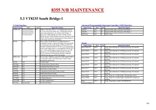
5.3 VT8235 South Br<strong>id</strong>ge-1<br />
V-Link Interface<br />
Signal Name Pin # I/O Signal Description<br />
VAD[15:0] K22,J22,G24,H22, IO Address /Data Bus. Bits 0-7 are implemented and bits<br />
G22,G23,F23,D25, 8-15 are reserved for future use. VAD[6:0]are used to<br />
K26,K24,E24,E26, send strap information o he chipset north br<strong>id</strong>ge. A<br />
J25,J26,F26,F25<br />
power up VAD[6:4]reflect he state of straps on pins<br />
SDA[2:0] and VAD[3:0]reflect the state of straps on pins<br />
SA[19:16].The specific interpretation of these straps is<br />
north br<strong>id</strong>ge chip design dependent.<br />
VPAR D26 IO Parity. If the VPAR function is implemented in a<br />
compatible manner on the north br<strong>id</strong>ge, this pin should<br />
be connected to the north br<strong>id</strong>ge VPAR pin (P4X333,<br />
P4X400, P4X800,KT400).If VPAR is not implemented<br />
in the north br<strong>id</strong>ge chip or is incompatible with he 8235<br />
(4x V-Link north br<strong>id</strong>ges) connect this pin to an 8.2K<br />
pull up to 2.5V (Pro266,Pro266T,KT266, KT266A,<br />
KT333, P4X266, PN266,KN266,KM266, P4M266,<br />
P4N266).See app note AN222 for details.<br />
VBE[1:0]# L26,F24 IO Byte Enables.VBE0#is used with VAD[7-0]and VBE1#<br />
is used with VAD[15-8](VBE1#and VAD[15-8]are<br />
reserved for future use).<br />
VCLK L24 I V-Link Clock.<br />
UPCMD K25 O Command from Client-to-Host.<br />
DNCMD J24 I Command from Host-to-Client.<br />
UPSTB H24 O Strobe from Client-to-Host.<br />
UPSTB# H26 O Complement Strobe from Client-to-Host.<br />
DNSTB G25 I Strobe from Host-to-Client.<br />
DNSTB# G26 I Complement Strobe from Host-to-Client.<br />
VLVREF J23 I Voltage Reference.<br />
VLCOMP K23 I V-Link Compensation.<br />
VCCVK (see pin list) P V-Link VK Power.<br />
8355 N/B MAINTENANCE<br />
Advanced Programmable Interrupt Controller (APIC)Interface<br />
Signal Name Pin # I/O Signal Description<br />
APICD1 V23 O Internal APIC Data 1.Function 0 Rx58[6]=1<br />
APICD0 T22 O Internal APIC Data 0.Function 0 Rx58[6]=1<br />
APICCLK U23 I APIC Clock.<br />
Straps<br />
Signal Name Pin # I/O Signal Description<br />
Strap /SDCS3# AD23 I Strap. State reflected on VAD[7]at powerup. No internal<br />
function.<br />
Strap /SDA2 AF23 I Strap. State reflected on VAD[6]at powerup. No internal<br />
function.<br />
Strap /SDA1 AC22 I Strap. State reflected on VAD[5]at powerup. No internal<br />
function.<br />
Strap /SDA0 AE23 I Strap. State reflected on VAD[4]at powerup. No internal<br />
function.<br />
Strap /SA19 AC11 I Strap. State reflected on VAD[3]at powerup. No internal<br />
function.<br />
Strap /SA18 AD11 I Strap. State reflected on VAD[2]at powerup. No internal<br />
function.<br />
Strap /SA17 AE11 I Strap. State reflected on VAD[1]at powerup. No internal<br />
function.<br />
Strap /SA16 AF11 I Strap. State reflected on VAD[0]at powerup. No internal<br />
function.<br />
Strap /SOE# AD12 I Strap. Strap low o enable (high o disable)<strong>au</strong>to reboot.<br />
Strap /SPKR AE9 I Strap. Strap low o enable (high o disable)CPU frequency s<br />
Strap<br />
/ROMCS#/KBCS#<br />
AF12 I<br />
rapping<br />
Strap. Strap high to enable LPCBIOSROM<br />
106