mitac 8355.pdf - tim.id.au
mitac 8355.pdf - tim.id.au
mitac 8355.pdf - tim.id.au

You also want an ePaper? Increase the reach of your titles
YUMPU automatically turns print PDFs into web optimized ePapers that Google loves.
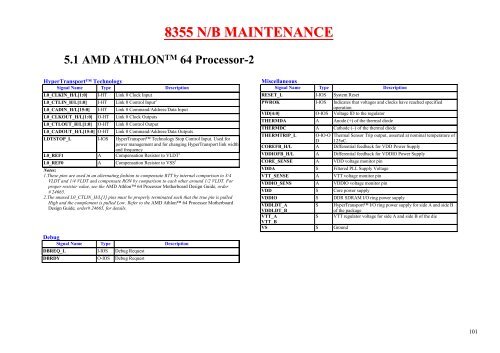
8355 N/B MAINTENANCE<br />
5.1 AMD ATHLON TM 64 Processor-2<br />
HyperTransport Technology<br />
Signal Name Type Description<br />
L0_CLKIN_H/L[1:0] I-HT Link 0 Clock Input<br />
L0_CTLIN_H/L[1:0] I-HT Link 0 Control Input 2<br />
L0_CADIN_H/L[15:0] I-HT Link 0 Command/Address/Data Input<br />
L0_CLKOUT_H/L[1:0] O-HT Link 0 Clock Outputs<br />
L0_CTLOUT_H/L[1:0] O-HT Link 0 Control Output<br />
L0_CADOUT_H/L[15:0] O-HT Link 0 Command/Address/Data Outputs<br />
LDTSTOP_L I-IOS HyperTransport Technology Stop Control Input. Used for<br />
power management and for changing HyperTransport link w<strong>id</strong>th<br />
and frequency<br />
L0_REF1 A Compensation Resistor to VLDT 1<br />
L0_REF0 A Compensation Resistor to VSS 1<br />
Notes:<br />
1.These pins are used in an alternating fashion to compensate RTT by internal comparison to 3/4<br />
VLDT and 1/4 VLDT and compensate RON by comparison to each other around 1/2 VLDT. For<br />
proper resistor value, see the AMD Athlon 64 Processor Motherboard Design Gu<strong>id</strong>e, order<br />
# 24665.<br />
2.The unused L0_CTLIN_H/L[1] pins must be properly terminated such that the true pin is pulled<br />
High and the complement is pulled Low. Refer to the AMD Athlon 64 Processor Motherboard<br />
Design Gu<strong>id</strong>e, order# 24665, for details.<br />
Debug<br />
Signal Name Type Description<br />
DBREQ_L I-IOS Debug Request<br />
DBRDY O-IOS Debug Request<br />
Miscellaneous<br />
Signal Name Type Description<br />
RESET_L I-IOS System Reset<br />
PWROK I-IOS Indicates that voltages and clocks have reached specified<br />
operation<br />
VID[4:0] O-IOS Voltage ID to the regulator<br />
THERMDA A Anode (+) of the thermal diode<br />
THERMDC A Cathode (–) of the thermal diode<br />
THERMTRIP_L O-IO-O Thermal Sensor Trip output, asserted at nominal temperature of<br />
D 125oC.<br />
COREFB_H/L A Differential feedback for VDD Power Supply<br />
VDDIOFB_H/L A Differential feedback for VDDIO Power Supply<br />
CORE_SENSE A VDD voltage monitor pin<br />
VDDA S Filtered PLL Supply Voltage<br />
VTT_SENSE A VTT voltage monitor pin<br />
VDDIO_SENS A VDDIO voltage monitor pin<br />
VDD S Core power supply<br />
VDDIO S DDR SDRAM I/O ring power supply<br />
VDDLDT_A<br />
S HyperTransport I/O ring power supply for s<strong>id</strong>e A and s<strong>id</strong>e B<br />
VDDLDT_B<br />
of the package<br />
VTT_A<br />
VTT_B<br />
S VTT regulator voltage for s<strong>id</strong>e A and s<strong>id</strong>e B of the die<br />
VS S Ground<br />
101