A Wavelength Converter Integrated with a Discretely Tunable Laser ...
A Wavelength Converter Integrated with a Discretely Tunable Laser ...
A Wavelength Converter Integrated with a Discretely Tunable Laser ...

Create successful ePaper yourself
Turn your PDF publications into a flip-book with our unique Google optimized e-Paper software.
94 7. MZI wavelength converter<br />
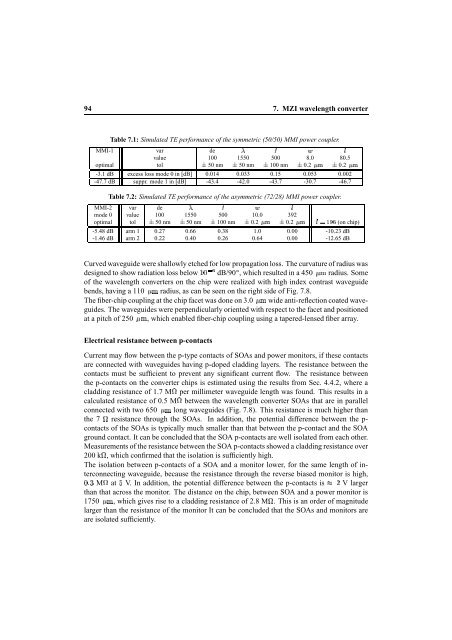
Table 7.1: Simulated TE performance of the symmetric (50/50) MMI power coupler.<br />
MMI-1 var de <br />
<br />
<br />
value 100 1550 500 8.0 80.5<br />
optimal tol 50 nm 50 nm 100 nm 0.2 0.2<br />
-3.1 dB excess loss mode 0 in [dB] 0.014 0.033 0.15 0.053 0.002<br />
-47.7 dB suppr. mode 1 in [dB] -43.4 -42.0 -43.7 -30.7 -46.7<br />
Table 7.2: Simulated TE performance of the asymmetric (72/28) MMI power coupler.<br />
MMI-2 var de <br />
© <br />
mode 0 value 100 1550 500 10.0 392<br />
optimal tol 50 nm 50 nm 100 nm 0.2 0.2 (on chip)<br />
-5.48 dB arm 1 0.27 0.66 0.38 1.0 0.00 -10.23 dB<br />
-1.46 dB arm 2 0.22 0.40 0.26 0.64 0.00 -12.65 dB<br />
Curved waveguide were shallowly etched for low propagation loss. The curvature of radius was<br />
designed to show radiation loss below ¤ dB/90 , which resulted in a 450 radius. Some<br />
of the wavelength converters on the chip were realized <strong>with</strong> high index contrast waveguide<br />
bends, having a 110 radius, as can be seen on the right side of Fig. 7.8.<br />
The fiber-chip coupling at the chip facet was done on 3.0 wide anti-reflection coated waveguides.<br />
The waveguides were perpendicularly oriented <strong>with</strong> respect to the facet and positioned<br />
at a pitch of 250 , which enabled fiber-chip coupling using a tapered-lensed fiber array.<br />
Electrical resistance between p-contacts<br />
Current may flow between the p-type contacts of SOAs and power monitors, if these contacts<br />
are connected <strong>with</strong> waveguides having p-doped cladding layers. The resistance between the<br />
contacts must be sufficient to prevent any significant current flow. The resistance between<br />
the p-contacts on the converter chips is estimated using the results from Sec. 4.4.2, where a<br />
cladding resistance of 1.7 M per millimeter waveguide length was found. This results in a<br />
calculated resistance of 0.5 M between the wavelength converter SOAs that are in parallel<br />
connected <strong>with</strong> two 650 long waveguides (Fig. 7.8). This resistance is much higher than<br />
the 7 resistance through the SOAs. In addition, the potential difference between the pcontacts<br />
of the SOAs is typically much smaller than that between the p-contact and the SOA<br />
ground contact. It can be concluded that the SOA p-contacts are well isolated from each other.<br />
Measurements of the resistance between the SOA p-contacts showed a cladding resistance over<br />
200 k , which confirmed that the isolation is sufficiently high.<br />
The isolation between p-contacts of a SOA and a monitor lower, for the same length of interconnecting<br />
waveguide, because the resistance through the reverse biased monitor is high,<br />
M at ¨ V. In addition, the potential difference between the p-contacts is § V larger<br />
than that across the monitor. The distance on the chip, between SOA and a power monitor is<br />
1750 , which gives rise to a cladding resistance of 2.8 M . This is an order of magnitude<br />
larger than the resistance of the monitor It can be concluded that the SOAs and monitors are<br />
are isolated sufficiently.