A Wavelength Converter Integrated with a Discretely Tunable Laser ...
A Wavelength Converter Integrated with a Discretely Tunable Laser ...
A Wavelength Converter Integrated with a Discretely Tunable Laser ...

You also want an ePaper? Increase the reach of your titles
YUMPU automatically turns print PDFs into web optimized ePapers that Google loves.
5.3 Waveguide processing 67<br />
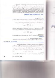
InP<br />
Q(1.25)<br />
InP<br />
First growth<br />
Second growth<br />
InP<br />
Q(1.25)<br />
InP<br />
First growth<br />
Second growth<br />
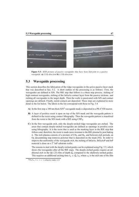
Figure 5.3: SEM pictures of passive waveguides that have been butt-joint to a passive<br />
waveguide. a) (110) direction b) (-110) direction<br />
5.3 Waveguide processing<br />
This section describes the fabrication of the ridge waveguides in the active-passive layer stack<br />
that was described in Sec. 5.2. A short outline of the processing is as follows: First, the<br />
waveguides are defined in SiN. The RIE step that follows is a three step process: etching of<br />
high contrast waveguides, etching of the InGaAs contact layer from the passive sections. and<br />
etching all waveguides to the target depth. Then the wafer is passivated <strong>with</strong> SiN and contact<br />
openings are defined. Finally, metal contacts are deposited. These steps are explained in more<br />
detail in the list below. The labels in the list correspond <strong>with</strong> those in Fig. 5.4.<br />
A) In the first step a 100 nm thick SiN waveguide mask is deposited in a PE-CVD reactor.<br />
B) A layer of positive resist is spun on top of the SiN mask and the waveguide pattern is<br />
defined in the resist using contact lithography. Then the waveguide pattern is transfered<br />
from the resist to the SiN mask <strong>with</strong> a RIE using CHF .<br />
C) In the first waveguide etch, only the deeply-etched ridge waveguides are etched. The<br />
areas that contain deeply-etched waveguides are defined as openings in positive resist<br />
using lithography. It is the resist that is used as the masking layer in the RIE step that<br />
follows and, therefore, the resist is made more resistant to the RIE plasma by post baking<br />
it. The etch plasma consists of a mixture of CH and H ¦ , and between etch periods, an<br />
O ¦ descumming step removes polymer that is deposited on the mask [92]. In order to<br />
improve the uniformity of the waveguide etch, the etching of InGaAs, InGaAsP and InP<br />
material is done on a 2” InP substrate wafer.<br />
The reasons to start <strong>with</strong> the deeply-etched guides can be explained using Fig. 5.5, which<br />
shows the waveguides after all the RIE steps. The deeply-etched guides require an additional<br />
etch in the Q(1.25) film of depth <br />
compared to the shallowly-etched guides.<br />
<br />
This requires an additional etching time <br />
is the etch rate of the film<br />
, , refractive index=2.0<br />
<br />
<br />
<br />
, where