A Wavelength Converter Integrated with a Discretely Tunable Laser ...
A Wavelength Converter Integrated with a Discretely Tunable Laser ...
A Wavelength Converter Integrated with a Discretely Tunable Laser ...
You also want an ePaper? Increase the reach of your titles
YUMPU automatically turns print PDFs into web optimized ePapers that Google loves.
5.4 Contact openings and metalization 73<br />
The definition of the contacts openings in the SiN isolation layer is normally done using contact<br />
lithography. A narrow opening in resist on top of the SOA is defined and in the next step the<br />
SiN in the opening is etched away. This is an increasingly difficult process if the SOA ridges<br />
become narrower (<br />
SOAs benefits from a self-aligned process. In the list below, four ways of fabricating contact<br />
openings on SOA ridges are compared. The first paragraph describes the standard method.<br />
The other three describe self-aligned methods.<br />
2.0 ), depending on the technology that is used. Therefore, narrow<br />
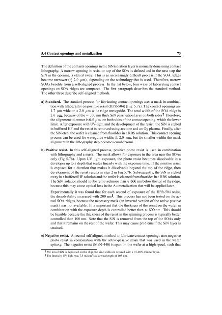
a) Standard. The standard process for fabricating contact openings uses a mask in combination<br />
<strong>with</strong> lithography on positive resist (HPR-504) (Fig. 5.7a). The contact openings are<br />
1.7 wide on a 2.0 wide ridge waveguide. The total width of the SOA ridge is<br />
2.6 , because of § the 300 nm thick SiN passivation layer on sides both Therefore,<br />
the alignment tolerance is 0.5 on both sides of the contact opening, which the lower<br />
limit. After exposure <strong>with</strong> UV-light and the development of the resist, the SiN is etched<br />
in buffered HF and the resist is removed using acetone and an ¦ O plasma. Finally, after<br />
the SiN etch, the wafer is cleaned from fluorides in a RBS solution. This contact opening<br />
process can be used for waveguide widths 2.0 , but for smaller widths the mask<br />
alignment in the lithography step becomes cumbersome.<br />
b) Positive resist. In this self-aligned process, positive photo resist is used in combination<br />
<strong>with</strong> lithography and a mask. The mask allows for exposure in the area near the SOAs<br />
only (Fig 5.7b). Upon UV light exposure, the photo resist becomes dissolvable in a<br />
developer up to a depth that scales linearly <strong>with</strong> the exposure time. If the positive resist<br />
is exposed for a duration that makes it dissolvable beyond the top of the ridge, then<br />
development of the resist results in step 2 in Fig 5.7b. Subsequently, the SiN is etched<br />
away in a buffered HF solution and the wafer is cleaned from fluorides in a RBS solution.<br />
The SiN isolation should not be removed more than § nm below the top of the ridge,<br />
because this may cause optical loss in the Au metalization that will be applied later.<br />
Experimentally it was found that for each second of exposure of the HPR-504 resist,<br />
the dissolvability increased <strong>with</strong> 200 nm . This process has not been tested on the actual<br />
SOA ridges, because the necessary mask (an inverted version of the active-passive<br />
mask) was not available. It is important that the thickness of the resist on the wafer in<br />
combination <strong>with</strong> the exposure depth is controlled better then § nm. This should<br />
be feasible because the thickness of the resist in the spinning process is typically better<br />
controlled than 100 nm. Note that the SiN is removed from the top of the SOAs only<br />
and that it remains on the rest of the wafer. This may cause problems if the SiN layer is<br />
strained.<br />
c) Negative resist. A second self aligned method to fabricate contact openings uses negative<br />
photo resist in combination <strong>with</strong> the active-passive mask that was used in the wafer<br />
epitaxy. The negative resist (MaN-440) is spun on the wafer at a high speed, such that<br />
350 nm of SiN is deposited on the chip, but side walls are covered <strong>with</strong> a 10-20% thinner layer.<br />
<br />
The intensity UV light was 7.5 mJ/cm s at a wavelength of 405 nm.


