A Wavelength Converter Integrated with a Discretely Tunable Laser ...
A Wavelength Converter Integrated with a Discretely Tunable Laser ...
A Wavelength Converter Integrated with a Discretely Tunable Laser ...

Create successful ePaper yourself
Turn your PDF publications into a flip-book with our unique Google optimized e-Paper software.
4.3 Waveguide components 41<br />
Table 4.1: Shown are several material properties of ¢ ¢ lattice matched to<br />
InP. The properties are expressed in the As fraction . is the elementary electron mass.<br />
electron [ mass ¨ ¤ ¦<br />
]<br />
heavy hole [ mass ¨ ¤ ¦<br />
]<br />
light hole [ mass ¤ ¦<br />
]<br />
bandgap energy ¤ ¤ ¦<br />
[eV]<br />
real refractive index ¤¨¨ ¤ ¤ <br />
at<br />
4.3 Waveguide components<br />
This section provides an overview of the geometry and features of the three types of waveguide<br />
components in the PICs: passive waveguides, SOAs, and phase modulators. A more<br />
quantitative description of the optimization of the components can be found in Sec. 4.4.<br />
4.3.1 Passive waveguides<br />
Passive waveguides can be employed as interconnecting waveguides between the different<br />
components on a chip, or for the construction of passive components like (de-)multiplexers and<br />
power couplers. Most important requirements for passive waveguides are low propagation loss,<br />
mono mode behavior, suitability for small radii of curvature, and polarization independence. A<br />
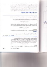
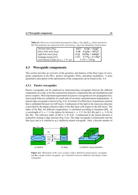
typical ridge waveguide is shown in Fig. 4.2a. It consists of a (film) layer of quaternary material<br />
that is embedded between two InP layers. Confinement of the light in the transverse direction<br />
is provided by the higher refractive index of the film layer <strong>with</strong> respect to the InP layers. The<br />
index of the film, for different compositions, is calculated according to Suematsu [68]. At<br />
a wavelength of ¤ ¨¨ the indices lie between for Q(1.00) and for<br />
Q(1.40). The refractive index of InP is ¤ . Confinement in the lateral direction is<br />
realized by etching a ridge structure (Fig. 4.2a). The ridge waveguide is etched partly into the<br />
film layer and it is referred to as a shallowly-etched waveguide. Only a discrete number of<br />
w<br />
opticall field<br />
InP<br />
Q( λg)<br />
film<br />
InP<br />
t f =<br />
500 nm<br />
w<br />
optical<br />
field<br />
a) shallow b) deep c) shallow−deep transition<br />
Figure 4.2: Illustration of the cross sections of a) a shallowly-etched passive waveguide<br />
and b) a deeply-etched waveguide. c) A Transition between shallowly and deeply etched<br />
waveguides.