Download complete software manual (PDF-File) - esd electronics, Inc.
Download complete software manual (PDF-File) - esd electronics, Inc.
Download complete software manual (PDF-File) - esd electronics, Inc.

Create successful ePaper yourself
Turn your PDF publications into a flip-book with our unique Google optimized e-Paper software.
ip<br />
tp (sample)<br />
op (input !)<br />
wr<br />
ar<br />
MSB<br />
LSB<br />
20<br />
A20<br />
A19<br />
A18<br />
A7<br />
A6<br />
A5<br />
Further parameters not shown:<br />
opol = 0<br />
tedg = 2<br />
A21 B1 B2 B3<br />
A21<br />
A20<br />
A19<br />
A8<br />
A7<br />
A6<br />
B1<br />
A21<br />
A20<br />
A9<br />
A8<br />
A7<br />
A21<br />
A20<br />
A19<br />
A8<br />
A7<br />
A6<br />
B2<br />
B1<br />
A21<br />
A10<br />
A9<br />
A8<br />
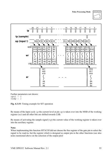
Fig. 4.3.15: Timing example for SIT operation<br />
B3<br />
B2<br />
B1<br />
A11<br />
A10<br />
A9<br />
B14<br />
B13<br />
B12<br />
B1<br />
A21<br />
A20<br />
Pulse Processing Mode<br />
21 1 2 3 14 15 16 17 18 1 2<br />
B14 B15 B16 B17 B18 C1<br />
By means of the input cycle ip the current level at pin op is taken over into the MSB of the working<br />
register (wr) and all other bits are shifted towards LSB.<br />
By means of activating the sample signal (tp) the current value of the working register is taken over<br />
into the auxiliary register.<br />
Note:<br />
When implementing this function HITACHI did not choose the free register of the gate pin to select the<br />
signal to be read-in, but the register which is designed as output pin in the other functions (see also<br />
notes mentioned above on the selection of the output pin)!<br />
VME DPIO32 Software Manual Rev. 2.1 55<br />
B15<br />
B14<br />
B13<br />
B2<br />
B1<br />
A21<br />
B16<br />
B15<br />
B14<br />
B3<br />
B2<br />
B1<br />
B17<br />
B16<br />
B15<br />
B4<br />
B3<br />
B2<br />
B18<br />
B17<br />
B16<br />
B5<br />
B4<br />
B3<br />
C1<br />
B18<br />
B17<br />
B6<br />
B5<br />
B4<br />
B18<br />
B17<br />
B16<br />
B5<br />
B4<br />
B3