Download complete software manual (PDF-File) - esd electronics, Inc.
Download complete software manual (PDF-File) - esd electronics, Inc.
Download complete software manual (PDF-File) - esd electronics, Inc.

You also want an ePaper? Increase the reach of your titles
YUMPU automatically turns print PDFs into web optimized ePapers that Google loves.
ip<br />
tp<br />
ar<br />
wr<br />
op<br />
MSB<br />
LSB<br />
20<br />
0<br />
0<br />
0<br />
0<br />
0<br />
0<br />
21 1 2 3 15 16 17 18 1<br />
B15<br />
B14<br />
B13<br />
B2<br />
B1<br />
B0<br />
0 B0<br />
0<br />
B15<br />
B14<br />
B3<br />
B2<br />
B1<br />
0<br />
0<br />
B15<br />
B4<br />
B3<br />
B2<br />
0<br />
0<br />
0<br />
B5<br />
B4<br />
B3<br />
0<br />
0<br />
B15<br />
C15<br />
C14<br />
C13<br />
C2<br />
C1<br />
C0<br />
0<br />
C15<br />
C14<br />
0 0 0 B0 B1 B2 B3 B14 B15 0 0 0 C0 C1<br />
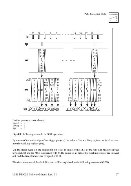
Further parameters not shown:<br />
opol = 0<br />
tedg = 2<br />
gp = 0<br />
Fig. 4.3.16: Timing example for SOT operation<br />
0<br />
0<br />
0<br />
0<br />
B15<br />
B14<br />
0<br />
0<br />
0<br />
0<br />
0<br />
0<br />
0<br />
0<br />
0<br />
Pulse Processing Mode<br />
By means of the active edge of the trigger pin (tp) the value of the auxiliary register ar is taken over<br />
into the working register (wr).<br />
Via the input cycle ip the output pin op is set to value of the LSB of the wr. The bits are shifted<br />
towards LSB and the MSB is assigned with '0'. By doing so all bits of the working register are 'moved<br />
out' and the free elements are assigned with '0'.<br />
VME DPIO32 Software Manual Rev. 2.1 57<br />
0<br />
0<br />
0<br />
0<br />
0<br />
0<br />
0 C0<br />
The determination of the shift direction will be explained in the following command (SPO).<br />
C3<br />
C2<br />
C1