Download complete software manual (PDF-File) - esd electronics, Inc.
Download complete software manual (PDF-File) - esd electronics, Inc.
Download complete software manual (PDF-File) - esd electronics, Inc.

Create successful ePaper yourself
Turn your PDF publications into a flip-book with our unique Google optimized e-Paper software.
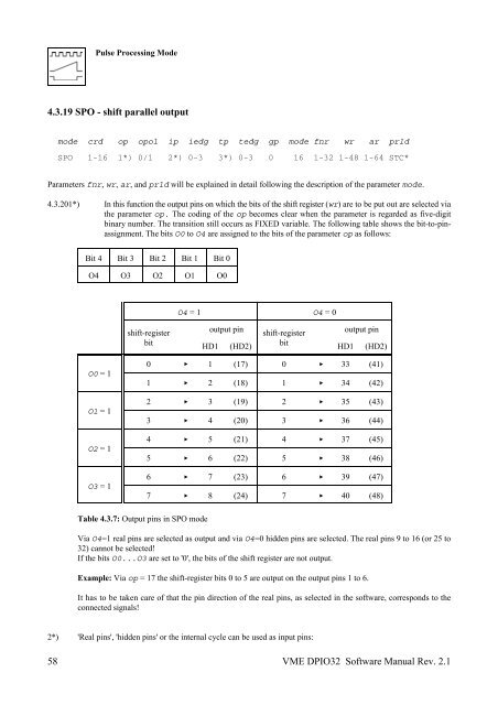
58<br />
Pulse Processing Mode<br />
4.3.19 SPO - shift parallel output<br />
+))))))H))))0))))0))))0))))0))))0))))0))))0))))0))))0))))0))))0))))0)))),<br />
* mode 5crd * op *opol* ip *iedg* tp *tedg* gp *mode*fnr * wr * ar *prld*<br />
G444444>4444P4444P4444P4444P4444P4444P4444P4444P4444P4444P4444P4444P4444I<br />
* SPO 51-16* 1*)*0/1 * 2*)*0-3 * 3*)*0-3 * 0 * 16 *1-32*1-48*1-64*STC**<br />
.))))))J))))2))))2))))2))))2))))2))))2))))2))))2))))2))))2))))2))))2))))-<br />
Parameters fnr, wr, ar, and prld will be explained in detail following the description of the parameter mode.<br />
4.3.201*) In this function the output pins on which the bits of the shift register (wr) are to be put out are selected via<br />
the parameter op. The coding of the op becomes clear when the parameter is regarded as five-digit<br />
binary number. The transition still occurs as FIXED variable. The following table shows the bit-to-pinassignment.<br />
The bits O0 to O4 are assigned to the bits of the parameter op as follows:<br />
Bit 4 Bit 3 Bit 2 Bit 1 Bit 0<br />
O4 O3 O2 O1 O0<br />
O0 = 1<br />
O1 = 1<br />
O2 = 1<br />
O3 = 1<br />
O4 = 1 O4 = 0<br />
shift-register<br />
output pin<br />
shift-register<br />
output pin<br />
bit<br />
HD1 (HD2)<br />
bit<br />
HD1 (HD2)<br />
Table 4.3.7: Output pins in SPO mode<br />
0 < 1 (17) 0 < 33 (41)<br />
1 < 2 (18) 1 < 34 (42)<br />
2 < 3 (19) 2 < 35 (43)<br />
3 < 4 (20) 3 < 36 (44)<br />
4 < 5 (21) 4 < 37 (45)<br />
5 < 6 (22) 5 < 38 (46)<br />
6 < 7 (23) 6 < 39 (47)<br />
7 < 8 (24) 7 < 40 (48)<br />
Via O4=1 real pins are selected as output and via O4=0 hidden pins are selected. The real pins 9 to 16 (or 25 to<br />
32) cannot be selected!<br />
If the bits O0...O3 are set to '0', the bits of the shift register are not output.<br />
Example: Via op = 17 the shift-register bits 0 to 5 are output on the output pins 1 to 6.<br />
It has to be taken care of that the pin direction of the real pins, as selected in the <strong>software</strong>, corresponds to the<br />
connected signals!<br />
2*) 'Real pins', 'hidden pins' or the internal cycle can be used as input pins:<br />
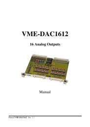
VME DPIO32 Software Manual Rev. 2.1