Laboratory Manual - King Fahd University of Petroleum and Minerals
Laboratory Manual - King Fahd University of Petroleum and Minerals
Laboratory Manual - King Fahd University of Petroleum and Minerals

You also want an ePaper? Increase the reach of your titles
YUMPU automatically turns print PDFs into web optimized ePapers that Google loves.
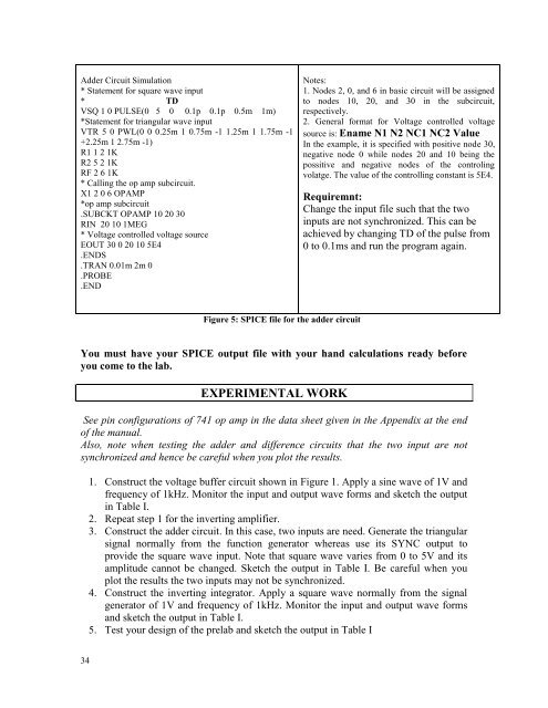
Adder Circuit Simulation<br />
* Statement for square wave input<br />
* TD<br />
VSQ 1 0 PULSE(0 5 0 0.1p 0.1p 0.5m 1m)<br />
*Statement for triangular wave input<br />
VTR 5 0 PWL(0 0 0.25m 1 0.75m -1 1.25m 1 1.75m -1<br />
+2.25m 1 2.75m -1)<br />
R1 1 2 1K<br />
R2 5 2 1K<br />
RF 2 6 1K<br />
* Calling the op amp subcircuit.<br />
X1 2 0 6 OPAMP<br />
*op amp subcircuit<br />
.SUBCKT OPAMP 10 20 30<br />
RIN 20 10 1MEG<br />
* Voltage controlled voltage source<br />
EOUT 30 0 20 10 5E4<br />
.ENDS<br />
.TRAN 0.01m 2m 0<br />
.PROBE<br />
.END<br />
Notes:<br />
1. Nodes 2, 0, <strong>and</strong> 6 in basic circuit will be assigned<br />
to nodes 10, 20, <strong>and</strong> 30 in the subcircuit,<br />
respectively.<br />
2. General format for Voltage controlled voltage<br />
source is: Ename N1 N2 NC1 NC2 Value<br />
In the example, it is specified with positive node 30,<br />
negative node 0 while nodes 20 <strong>and</strong> 10 being the<br />
possitive <strong>and</strong> negative nodes <strong>of</strong> the controling<br />
volatge. The value <strong>of</strong> the controlling constant is 5E4.<br />
Requiremnt:<br />
Change the input file such that the two<br />
inputs are not synchronized. This can be<br />
achieved by changing TD <strong>of</strong> the pulse from<br />
0 to 0.1ms <strong>and</strong> run the program again.<br />
Figure 5: SPICE file for the adder circuit<br />
You must have your SPICE output file with your h<strong>and</strong> calculations ready before<br />
you come to the lab.<br />
EXPERIMENTAL WORK<br />
See pin configurations <strong>of</strong> 741 op amp in the data sheet given in the Appendix at the end<br />
<strong>of</strong> the manual.<br />
Also, note when testing the adder <strong>and</strong> difference circuits that the two input are not<br />
synchronized <strong>and</strong> hence be careful when you plot the results.<br />
1. Construct the voltage buffer circuit shown in Figure 1. Apply a sine wave <strong>of</strong> 1V <strong>and</strong><br />
frequency <strong>of</strong> 1kHz. Monitor the input <strong>and</strong> output wave forms <strong>and</strong> sketch the output<br />
in Table I.<br />
2. Repeat step 1 for the inverting amplifier.<br />
3. Construct the adder circuit. In this case, two inputs are need. Generate the triangular<br />
signal normally from the function generator whereas use its SYNC output to<br />
provide the square wave input. Note that square wave varies from 0 to 5V <strong>and</strong> its<br />
amplitude cannot be changed. Sketch the output in Table I. Be careful when you<br />
plot the results the two inputs may not be synchronized.<br />
4. Construct the inverting integrator. Apply a square wave normally from the signal<br />
generator <strong>of</strong> 1V <strong>and</strong> frequency <strong>of</strong> 1kHz. Monitor the input <strong>and</strong> output wave forms<br />
<strong>and</strong> sketch the output in Table I.<br />
5. Test your design <strong>of</strong> the prelab <strong>and</strong> sketch the output in Table I<br />
34