Spin-orbit coupling and electron-phonon scattering - Fachbereich ...
Spin-orbit coupling and electron-phonon scattering - Fachbereich ...
Spin-orbit coupling and electron-phonon scattering - Fachbereich ...
You also want an ePaper? Increase the reach of your titles
YUMPU automatically turns print PDFs into web optimized ePapers that Google loves.
54 Rashba spin-<strong>orbit</strong> <strong>coupling</strong> in quantum dots<br />
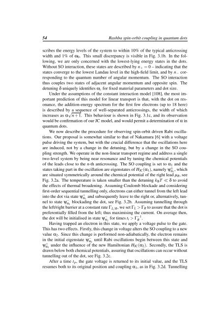
scribes the energy levels of the system to within 10% of the typical anticrossing<br />
width <strong>and</strong> 1% of ω 0 . This small discrepancy is visible in Fig. 3.1b. In the following,<br />
we are only concerned with the lowest-lying energy states in the dots.<br />
Without SO interaction, these states are described by n + = 0 – indicating that the<br />
states converge to the lowest L<strong>and</strong>au level in the high-field limit, <strong>and</strong> by n − corresponding<br />
to the quantum number of angular momentum. The SO interaction<br />
thus couples two states of adjacent angular momentum <strong>and</strong> opposite spin. The<br />
detuning δ uniquely identifies ω c for fixed material parameters <strong>and</strong> dot size.<br />
Under the assumptions of the constant interaction model [108], the most important<br />
prediction of this model for linear transport is that, with the dot on resonance,<br />
the addition-energy spectrum for the first few <strong>electron</strong>s (up to 18 here)<br />
is described by a sequence of well-separated anticrossings, the width of which<br />
increases as α √ n + 1. This behaviour is shown in Fig. 3.1c, <strong>and</strong> its observation<br />
would be confirmation of our JC model, <strong>and</strong> would permit a determination of α in<br />
quantum dots.<br />
We now describe the procedure for observing spin-<strong>orbit</strong> driven Rabi oscillations.<br />
Our proposal is somewhat similar to that of Nakamura [6] with a voltage<br />
pulse driving the system, but with the crucial difference that the oscillations here<br />
are induced, not by a change in the detuning, but by a change in the SO <strong>coupling</strong><br />
strength. We operate in the non-linear transport regime <strong>and</strong> address a single<br />
two-level system by being near resonance <strong>and</strong> by tuning the chemical potentials<br />
of the leads close to the n-th anticrossing. The SO <strong>coupling</strong> is set to α 1 <strong>and</strong> the<br />
states taking part in the oscillation are eigenstates of H JC (α 1 ), namely ψ ± α 1<br />
, which<br />
are situated symmetrically around the chemical potential of the right lead µ R , see<br />
Fig. 3.2a. The temperature is taken smaller than the detuning k B T ≪ δ to avoid<br />
the effects of thermal broadening. Assuming Coulomb blockade <strong>and</strong> considering<br />
first-order sequential tunnelling only, <strong>electron</strong>s can either tunnel from the left lead<br />
into the dot via state ψ + α 1<br />
<strong>and</strong> subsequently leave to the right or, alternatively, tunnel<br />
to state ψ − α 1<br />
blockading the dot, see Fig. 3.2b. Assuming tunnelling through<br />
the left/right barrier at a constant rate Γ L/R , we set Γ L > Γ R to assure that the dot is<br />
preferentially filled from the left; thus maximising the current. On average then,<br />
the dot will be initialised in state ψ − α 1<br />
for times t i > Γ −1<br />
R .<br />
Having trapped an <strong>electron</strong> in this state, we apply a voltage pulse to the gate.<br />
This has two effects. Firstly, this change in voltage alters the SO <strong>coupling</strong> to a new<br />
value α 2 . Since this change is performed non-adiabatically, the <strong>electron</strong> remains<br />
in the initial eigenstate ψ − α 1<br />
until Rabi oscillations begin between this state <strong>and</strong><br />
ψ + α 1<br />
under the influence of the new Hamiltonian H JC (α 2 ). Secondly, the TLS is<br />
drawn below both chemical potentials, assuring that oscillations can occur without<br />
tunnelling out of the dot, see Fig. 3.2c.<br />
After a time t p , the gate voltage is returned to its initial value, <strong>and</strong> the TLS<br />
resumes both to its original position <strong>and</strong> <strong>coupling</strong> α 1 , as in Fig. 3.2d. Tunnelling


