

digital compensation of dynamic acquisition errors at the front-end of ...
digital compensation of dynamic acquisition errors at the front-end of ...
digital compensation of dynamic acquisition errors at the front-end of ...

You also want an ePaper? Increase the reach of your titles
YUMPU automatically turns print PDFs into web optimized ePapers that Google loves.
18 Chapter 2: Nonlinearity <strong>at</strong> <strong>the</strong> ADC’s Front-End<br />
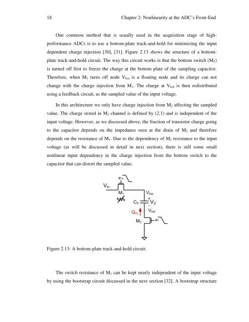
One common method th<strong>at</strong> is usually used in <strong>the</strong> <strong>acquisition</strong> stage <strong>of</strong> highperformance<br />
ADCs is to use a bottom-pl<strong>at</strong>e track-and-hold for minimizing <strong>the</strong> input<br />
dep<strong>end</strong>ent charge injection [30], [31]. Figure 2.13 shows <strong>the</strong> structure <strong>of</strong> a bottompl<strong>at</strong>e<br />
track-and-hold circuit. The way this circuit works is th<strong>at</strong> <strong>the</strong> bottom switch (M 2 )<br />
is turned <strong>of</strong>f first to freeze <strong>the</strong> charge <strong>at</strong> <strong>the</strong> bottom pl<strong>at</strong>e <strong>of</strong> <strong>the</strong> sampling capacitor.<br />
Therefore, when M 1 turns <strong>of</strong>f node V bot is a flo<strong>at</strong>ing node and its charge can not<br />
change with <strong>the</strong> charge injection from M 1 . The charge <strong>at</strong> V bot is <strong>the</strong>n redistributed<br />
using a feedback circuit, as <strong>the</strong> sampled value <strong>of</strong> <strong>the</strong> input voltage.<br />
In this architecture we only have charge injection from M 2 affecting <strong>the</strong> sampled<br />
value. The charge stored in M 2 channel is defined by (2.1) and is indep<strong>end</strong>ent <strong>of</strong> <strong>the</strong><br />
input voltage. However, as we discussed above, <strong>the</strong> fraction <strong>of</strong> transistor charge going<br />
to <strong>the</strong> capacitor dep<strong>end</strong>s on <strong>the</strong> impedance seen <strong>at</strong> <strong>the</strong> drain <strong>of</strong> M 2 and <strong>the</strong>refore<br />
dep<strong>end</strong>s on <strong>the</strong> resistance <strong>of</strong> M 1 . Due to <strong>the</strong> dep<strong>end</strong>ency <strong>of</strong> M 1 resistance to <strong>the</strong> input<br />
voltage (as will be discussed in detail in next section), <strong>the</strong>re is still some small<br />
nonlinear input dep<strong>end</strong>ency in <strong>the</strong> charge injection from <strong>the</strong> bottom switch to <strong>the</strong><br />
capacitor th<strong>at</strong> can distort <strong>the</strong> sampled value.<br />
φ 1d<br />
φ 1<br />
V in<br />
+<br />
V top<br />
M 1<br />
M 2<br />
C S<br />
Q inj<br />
-<br />
V C<br />
V bot<br />
Figure 2.13: A bottom-pl<strong>at</strong>e track-and-hold circuit.<br />
The switch resistance <strong>of</strong> M 1 can be kept nearly indep<strong>end</strong>ent <strong>of</strong> <strong>the</strong> input voltage<br />
by using <strong>the</strong> bootstrap circuit discussed in <strong>the</strong> next section [32]. A bootstrap structure


