digital compensation of dynamic acquisition errors at the front-end of ...
digital compensation of dynamic acquisition errors at the front-end of ...
digital compensation of dynamic acquisition errors at the front-end of ...
You also want an ePaper? Increase the reach of your titles
YUMPU automatically turns print PDFs into web optimized ePapers that Google loves.
22 Chapter 2: Nonlinearity <strong>at</strong> <strong>the</strong> ADC’s Front-End<br />
2.3.2 Nonlinearity in <strong>the</strong> tracking phase<br />
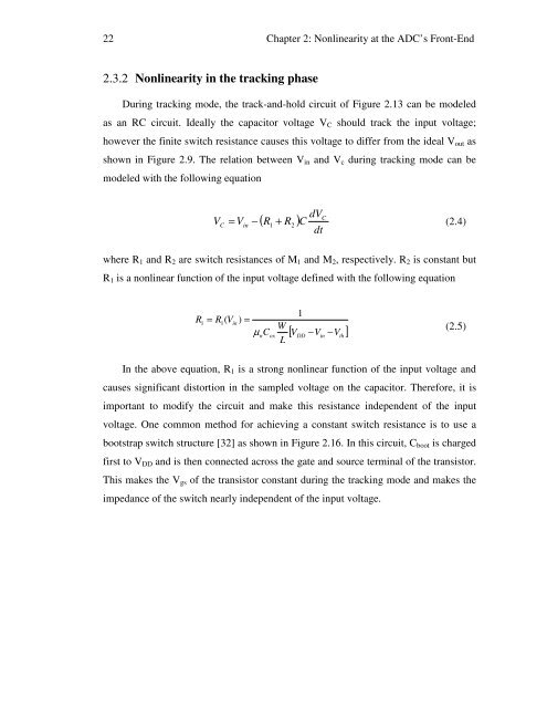
During tracking mode, <strong>the</strong> track-and-hold circuit <strong>of</strong> Figure 2.13 can be modeled<br />
as an RC circuit. Ideally <strong>the</strong> capacitor voltage V C should track <strong>the</strong> input voltage;<br />
however <strong>the</strong> finite switch resistance causes this voltage to differ from <strong>the</strong> ideal V out as<br />
shown in Figure 2.9. The rel<strong>at</strong>ion between V in and V c during tracking mode can be<br />
modeled with <strong>the</strong> following equ<strong>at</strong>ion<br />
V<br />
dVC<br />
= Vin<br />
− ( R1 + R ) C<br />
(2.4)<br />
dt<br />
C 2<br />
where R 1 and R 2 are switch resistances <strong>of</strong> M 1 and M 2 , respectively. R 2 is constant but<br />
R 1 is a nonlinear function <strong>of</strong> <strong>the</strong> input voltage defined with <strong>the</strong> following equ<strong>at</strong>ion<br />
R1<br />
= R1(<br />
Vin<br />
) =<br />
µ C<br />
n<br />
ox<br />
W<br />
L<br />
1<br />
[ V −V<br />
−V<br />
]<br />
DD<br />
in<br />
th<br />
(2.5)<br />
In <strong>the</strong> above equ<strong>at</strong>ion, R 1 is a strong nonlinear function <strong>of</strong> <strong>the</strong> input voltage and<br />
causes significant distortion in <strong>the</strong> sampled voltage on <strong>the</strong> capacitor. Therefore, it is<br />
important to modify <strong>the</strong> circuit and make this resistance indep<strong>end</strong>ent <strong>of</strong> <strong>the</strong> input<br />
voltage. One common method for achieving a constant switch resistance is to use a<br />
bootstrap switch structure [32] as shown in Figure 2.16. In this circuit, C boot is charged<br />
first to V DD and is <strong>the</strong>n connected across <strong>the</strong> g<strong>at</strong>e and source terminal <strong>of</strong> <strong>the</strong> transistor.<br />
This makes <strong>the</strong> V gs <strong>of</strong> <strong>the</strong> transistor constant during <strong>the</strong> tracking mode and makes <strong>the</strong><br />
impedance <strong>of</strong> <strong>the</strong> switch nearly indep<strong>end</strong>ent <strong>of</strong> <strong>the</strong> input voltage.


