

digital compensation of dynamic acquisition errors at the front-end of ...
digital compensation of dynamic acquisition errors at the front-end of ...
digital compensation of dynamic acquisition errors at the front-end of ...

You also want an ePaper? Increase the reach of your titles
YUMPU automatically turns print PDFs into web optimized ePapers that Google loves.
30 Chapter 2: Nonlinearity <strong>at</strong> <strong>the</strong> ADC’s Front-End<br />
a linear function with memory which is still comp<strong>at</strong>ible with our initial model<br />
(equ<strong>at</strong>ion (2.8)).<br />
Vin ( k)<br />
= fnonlin<br />
( Vout<br />
( k))<br />
× flin<br />
( Vout<br />
( k),<br />
Vout<br />
( k −1),<br />
Vout<br />
( k + 1),...) (2.10)<br />
where f nonlin is <strong>the</strong> result <strong>of</strong> RC product and f lin is gener<strong>at</strong>ed from different deriv<strong>at</strong>ive<br />
orders.<br />
Dep<strong>end</strong>ing on <strong>the</strong> initial voltages on <strong>the</strong> capacitors <strong>the</strong> response <strong>of</strong> this system to<br />
a sinusoidal input voltage can be shown as<br />
t<br />
−<br />
t<br />
−<br />
τ1 τ 2<br />
Vout 2<br />
= k1e<br />
+ k2e<br />
+ Asin(<br />
ωt<br />
+ ϕ)<br />
(2.11)<br />
where τ 1 and τ 2 are time constants <strong>of</strong> <strong>the</strong> circuit and k 1 and k 2 are defined based on<br />
initial voltages and <strong>the</strong> input sinewave. This shows th<strong>at</strong> <strong>the</strong> output voltage has a<br />
transient response first, before reaching <strong>the</strong> steady-st<strong>at</strong>e sinewave response. If this<br />
transient has not settled completely by <strong>the</strong> time <strong>of</strong> <strong>the</strong> sampling, it causes dep<strong>end</strong>ency<br />
to V out (n-1) in <strong>the</strong> nonlinear part <strong>of</strong> <strong>the</strong> output voltage.<br />
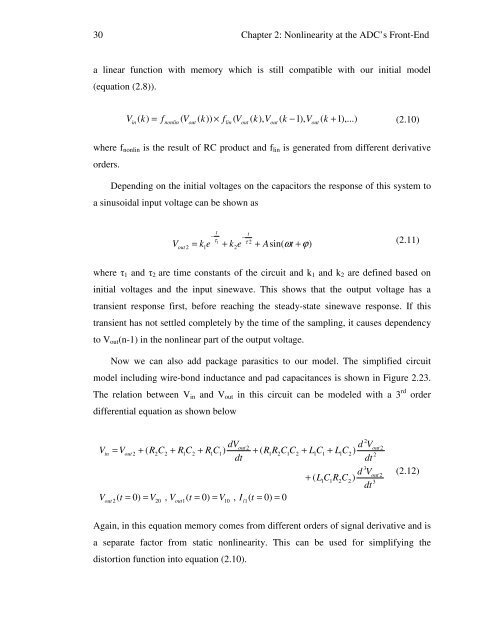
Now we can also add package parasitics to our model. The simplified circuit<br />
model including wire-bond inductance and pad capacitances is shown in Figure 2.23.<br />
The rel<strong>at</strong>ion between V in and V out in this circuit can be modeled with a 3 rd order<br />
differential equ<strong>at</strong>ion as shown below<br />
V<br />
V<br />
in<br />
out 2<br />
= V<br />
out 2<br />
+ ( R C<br />
2<br />
( t = 0) = V<br />
20<br />
2<br />
+ R C<br />
, V<br />
1<br />
out1<br />
2<br />
dV<br />
+ R1C<br />
1)<br />
dt<br />
( t = 0) = V<br />
10<br />
out 2<br />
, I<br />
l1<br />
+ ( R R C C<br />
1<br />
2<br />
( t = 0) = 0<br />
1<br />
2<br />
2<br />
d V<br />
+ L1C<br />
1<br />
+ L1C<br />
2)<br />
dt<br />
3<br />
d V<br />
+ ( L1C 1R2C2<br />
)<br />
dt<br />
out 2<br />
2<br />
out 2<br />
3<br />
(2.12)<br />
Again, in this equ<strong>at</strong>ion memory comes from different orders <strong>of</strong> signal deriv<strong>at</strong>ive and is<br />
a separ<strong>at</strong>e factor from st<strong>at</strong>ic nonlinearity. This can be used for simplifying <strong>the</strong><br />
distortion function into equ<strong>at</strong>ion (2.10).


