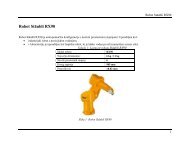
ARM Processor Instruction Set
ARM Processor Instruction Set
ARM Processor Instruction Set

Create successful ePaper yourself
Turn your PDF publications into a flip-book with our unique Google optimized e-Paper software.
<strong>ARM</strong> <strong>Processor</strong> <strong>Instruction</strong> <strong>Set</strong><br />
5.7.1 Offsets and auto-indexing<br />
The offset from the base may be either a 12-bit unsigned binary immediate value in<br />
the instruction, or a second register (possibly shifted in some way). The offset may be<br />
added to (U=1) or subtracted from (U=0) the base register Rn. The offset modification<br />
may be performed either before (pre-indexed, P=1) or after (post-indexed, P=0) the<br />
base is used as the transfer address.<br />
The W bit gives optional auto increment and decrement addressing modes.<br />
The modified base value may be written back into the base (W=1), or the old base<br />
value may be kept (W=0).<br />
Post-indexed addressing<br />
In the case of post-indexed addressing, the write back bit is redundant and is always<br />
set to zero, since the old base value can be retained by setting the offset to zero.<br />
Therefore post-indexed data transfers always write back the modified base. The only<br />
use of the W bit in a post-indexed data transfer is in privileged mode code, where<br />
setting the W bit forces non-privileged mode for the transfer, allowing the operating<br />
system to generate a user address in a system where the memory management<br />
hardware makes suitable use of this hardware.<br />
Preliminary - Unrestricted<br />
5.7.2 Shifted register offset<br />
5.7.3 Bytes and words<br />
The 8 shift control bits are described in the data processing instructions section.<br />
However, the register specified shift amounts are not available in this instruction class.<br />
See ➲5.4.2 Shifts on page 5-9.<br />
This instruction class may be used to transfer a byte (B=1) or a word (B=0) between<br />
an <strong>ARM</strong> processor register and memory. The following text assumes that the<br />
<strong>ARM</strong>7500 is operating with 32-bit wide memory. If it is operating with 16-bit wide<br />
memory, the positions of bytes on the external data bus will be different, although, on<br />
the <strong>ARM</strong>7500 internal data bus the positions will be as described here.<br />
The action of LDR(B) and STR(B) instructions is influenced by the 3 instruction<br />
fetches. For more information see ➲5.16.7 <strong>Instruction</strong> speed summary on page 5-55.<br />
The two possible configurations are described below.<br />
5-24<br />
<strong>ARM</strong>7500 Data Sheet<br />
<strong>ARM</strong> DDI 0050C