

PowerPC 740 and PowerPC 750 Microprocessor Datasheet - IBM
PowerPC 740 and PowerPC 750 Microprocessor Datasheet - IBM
PowerPC 740 and PowerPC 750 Microprocessor Datasheet - IBM
- No tags were found...

Create successful ePaper yourself
Turn your PDF publications into a flip-book with our unique Google optimized e-Paper software.
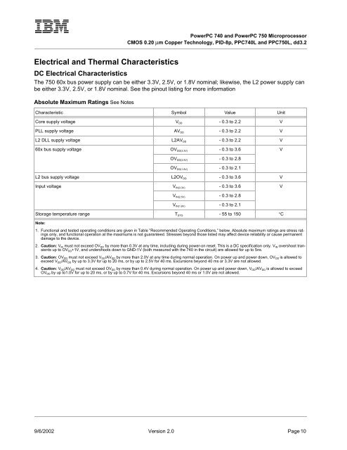
<strong>PowerPC</strong> <strong>740</strong> <strong>and</strong> <strong>PowerPC</strong> <strong>750</strong> <strong>Microprocessor</strong>CMOS 0.20 µm Copper Technology, PID-8p, PPC<strong>740</strong>L <strong>and</strong> PPC<strong>750</strong>L, dd3.2Electrical <strong>and</strong> Thermal CharacteristicsDC Electrical CharacteristicsThe <strong>750</strong> 60x bus power supply can be either 3.3V, 2.5V, or 1.8V nominal; likewise, the L2 power supply canbe either 3.3V, 2.5V, or 1.8V nominal. See the pinout listing for more informationAbsolute Maximum Ratings See NotesCharacteristic Symbol Value UnitCore supply voltage V DD - 0.3 to 2.2 VPLL supply voltage AV DD - 0.3 to 2.2 VL2 DLL supply voltage L2AV DD - 0.3 to 2.2 V60x bus supply voltage OV DD(3.3V) - 0.3 to 3.6 VOV DD(2.5V) - 0.3 to 2.8OV DD(1.8V) - 0.3 to 2.1L2 bus supply voltage L2OV DD - 0.3 to 3.6 VInput voltage V IN(3.3V) - 0.3 to 3.6 VV IN(2.5V) - 0.3 to 2.8V IN(1.8V) - 0.3 to 2.1Storage temperature range T STG - 55 to 150 °CNote:1. Functional <strong>and</strong> tested operating conditions are given in Table ”Recommended Operating Conditions,” below. Absolute maximum ratings are stress ratingsonly, <strong>and</strong> functional operation at the maximums is not guaranteed. Stresses beyond those listed may affect device reliability or cause permanentdamage to the device.2. Caution: V IN must not exceed OV DD by more than 0.3V at any time, including during power-on reset. This is a DC specification only. V IN overshoot transientsup to OV DD +1V, <strong>and</strong> undershoots down to GND-1V (both measured with the <strong>740</strong> in the circuit) are allowed for up to 5ns.3. Caution: OV DD must not exceed V DD /AV DD by more than 2.0V at any time during normal operation. On power up <strong>and</strong> power down, OV DD is allowed toexceed V DD /AV DD by up to 3.3V for up to 20 ms, or by up to 2.5V for 40 ms. Excursions beyond 40 ms or 3.3V are not allowed.4. Caution: V DD /AV DD must not exceed OV DD by more than 0.4V during normal operation. On power up <strong>and</strong> power down, V DD /AV DD is allowed to exceedOV DD by up to1.0V for up to 20 ms, or by up to 0.7V for 40 ms. Excursions beyond 40 ms or 1.0V are not allowed.9/6/2002 Version 2.0 Page 10


