

PowerPC 740 and PowerPC 750 Microprocessor Datasheet - IBM
PowerPC 740 and PowerPC 750 Microprocessor Datasheet - IBM
PowerPC 740 and PowerPC 750 Microprocessor Datasheet - IBM
- No tags were found...

You also want an ePaper? Increase the reach of your titles
YUMPU automatically turns print PDFs into web optimized ePapers that Google loves.
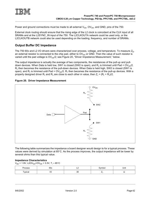
<strong>PowerPC</strong> <strong>740</strong> <strong>and</strong> <strong>PowerPC</strong> <strong>750</strong> <strong>Microprocessor</strong>CMOS 0.20 µm Copper Technology, PID-8p, PPC<strong>740</strong>L <strong>and</strong> PPC<strong>750</strong>L, dd3.2Power <strong>and</strong> ground connections must be made to all external V DD , OV DD , <strong>and</strong> GND, pins of the <strong>750</strong>.External clock routing should ensure that the rising edge of the L2 clock is coincident at the CLK input of allSRAMs <strong>and</strong> at the L2SYNC_IN input of the <strong>750</strong>. The L2CLKOUTA network could be used only, or theL2CLKOUTB network could also be used depending on the loading, frequency, <strong>and</strong> number of SRAMs.Output Buffer DC ImpedanceThe <strong>750</strong> 60x <strong>and</strong> L2 I/O drivers were characterized over process, voltage, <strong>and</strong> temperature. To measure Z 0 ,an external resistor is connected to the chip pad, either to OV DD or GND. Then the value of such resistor isvaried until the pad voltage is OV DD /2; see Figure 20, “Driver Impedance Measurement,” below.The output impedance is actually the average of two components, the resistances of the pull-up <strong>and</strong> pulldowndevices. When Data is held low, SW1 is closed (SW2 is open), <strong>and</strong> R N is trimmed until Pad = OV DD /2.R N then becomes the resistance of the pull-down devices. When Data is held high, SW2 is closed (SW1 isopen), <strong>and</strong> R P is trimmed until Pad = OV DD /2. R P then becomes the resistance of the pull-up devices. With aproperly designed driver R P <strong>and</strong> R N are close to each other in value, then Z 0 = (R P + R N )/2.Figure 20. Driver Impedance MeasurementOV DDR NSW2DataPadSW1R PGNDThe following table summarizes the impedance a board designer would design to for a typical process. Thesevalues were derived by simulation at 65°C. As the process improves, the output impedance will be lower byseveral ohms than this typical value.Impedance CharacteristicsV DD = 1.9V, L2OV DD =OV DD = 3.3V, T J = 65°CProcess 60x L2 Symbol UnitTypical 43 38 Z 0 Ω9/6/2002 Version 2.0 Page 42


