

PowerPC 740 and PowerPC 750 Microprocessor Datasheet - IBM
PowerPC 740 and PowerPC 750 Microprocessor Datasheet - IBM
PowerPC 740 and PowerPC 750 Microprocessor Datasheet - IBM
- No tags were found...

You also want an ePaper? Increase the reach of your titles
YUMPU automatically turns print PDFs into web optimized ePapers that Google loves.
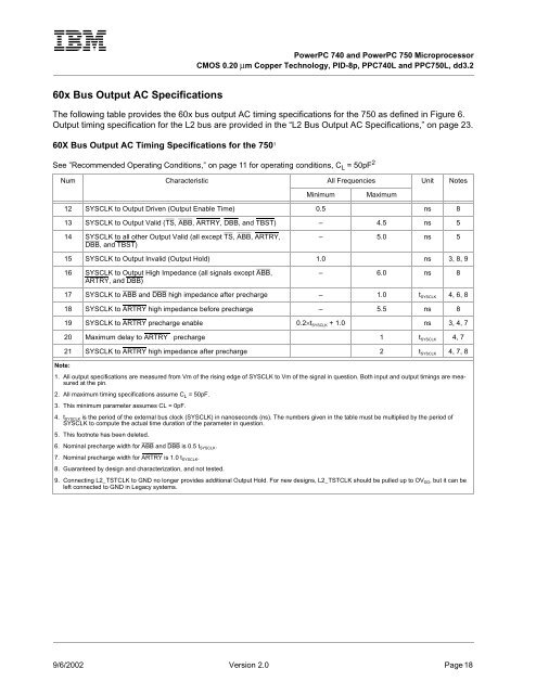
<strong>PowerPC</strong> <strong>740</strong> <strong>and</strong> <strong>PowerPC</strong> <strong>750</strong> <strong>Microprocessor</strong>CMOS 0.20 µm Copper Technology, PID-8p, PPC<strong>740</strong>L <strong>and</strong> PPC<strong>750</strong>L, dd3.260x Bus Output AC SpecificationsThe following table provides the 60x bus output AC timing specifications for the <strong>750</strong> as defined in Figure 6.Output timing specification for the L2 bus are provided in the “L2 Bus Output AC Specifications,” on page 23.60X Bus Output AC Timing Specifications for the <strong>750</strong> 1See ”Recommended Operating Conditions,” on page 11 for operating conditions, C L = 50pF 2Num Characteristic All Frequencies Unit NotesMinimumMaximum12 SYSCLK to Output Driven (Output Enable Time) 0.5 ns 813 SYSCLK to Output Valid (TS, ABB, ARTRY, DBB, <strong>and</strong> TBST) – 4.5 ns 514 SYSCLK to all other Output Valid (all except TS, ABB, ARTRY,DBB, <strong>and</strong> TBST)– 5.0 ns 515 SYSCLK to Output Invalid (Output Hold) 1.0 ns 3, 8, 916 SYSCLK to Output High Impedance (all signals except ABB,ARTRY, <strong>and</strong> DBB)– 6.0 ns 817 SYSCLK to ABB <strong>and</strong> DBB high impedance after precharge – 1.0 t SYSCLK 4, 6, 818 SYSCLK to ARTRY high impedance before precharge – 5.5 ns 819 SYSCLK to ARTRY precharge enable 0.2×t SYSCLK + 1.0 ns 3, 4, 720 Maximum delay to ARTRY precharge 1 t SYSCLK 4, 721 SYSCLK to ARTRY high impedance after precharge 2 t SYSCLK 4, 7, 8Note:1. All output specifications are measured from Vm of the rising edge of SYSCLK to Vm of the signal in question. Both input <strong>and</strong> output timings are measuredat the pin.2. All maximum timing specifications assume C L = 50pF.3. This minimum parameter assumes CL = 0pF.4. t SYSCLK is the period of the external bus clock (SYSCLK) in nanoseconds (ns). The numbers given in the table must be multiplied by the period ofSYSCLK to compute the actual time duration of the parameter in question.5. This footnote has been deleted.6. Nominal precharge width for ABB <strong>and</strong> DBB is 0.5 t SYSCLK .7. Nominal precharge width for ARTRY is 1.0 t SYSCLK .8. Guaranteed by design <strong>and</strong> characterization, <strong>and</strong> not tested.9. Connecting L2_TSTCLK to GND no longer provides additional Output Hold. For new designs, L2_TSTCLK should be pulled up to OV DD , but it can beleft connected to GND in Legacy systems.9/6/2002 Version 2.0 Page 18


