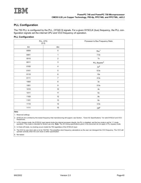
<strong>PowerPC</strong> <strong>740</strong> <strong>and</strong> <strong>PowerPC</strong> <strong>750</strong> <strong>Microprocessor</strong>CMOS 0.20 µm Copper Technology, PID-8p, PPC<strong>740</strong>L <strong>and</strong> PPC<strong>750</strong>L, dd3.2PLL ConfigurationThe <strong>750</strong> PLL is configured by the PLL_CFG[0:3] signals. For a given SYSCLK (bus) frequency, the PLL configurationsignals set the internal CPU <strong>and</strong> VCO frequency of operation.PLL ConfigurationPLL_CFG(0:3)Processor to Bus Frequency Ratiobindec0000 0 Rsv 10001 1 7.5x0010 2 7x0011 3 PLL Bypass 30100 4 2x 60101 5 6.5x0110 6 10x0111 7 4.5x1000 8 3x1001 9 5.5x10¹⁰ 10 4x10¹¹ 11 5x1100 12 8x1101 13 6x1110 14 3.5x1111 15 Off 4Note:1. Reserved settings.2. SYSCLK min is limited by the lowest frequency that manufacturing will support, see Section , “Clock AC Specifications,” for valid SYSCLK <strong>and</strong> VCOfrequencies.3. In PLL-bypass mode, the SYSCLK input signal clocks the internal processor directly, the PLL is disabled, <strong>and</strong> the bus mode is set for 1:1 modeoperation. This mode is intended for factory use only. Note: The AC timing specifications given in the document do not apply in PLL-bypass mode.4. In Clock-off mode, no clocking occurs inside the <strong>750</strong> regardless of the SYSCLK input.5. The VCO to core clock ratio is 2x for <strong>740</strong>/<strong>750</strong>. This simplifies clock frequency calculations so the user can disregard the VCO frequency. The VCO willoperate correctly when the core clock is within specification.6. Not tested.9/6/2002 Version 2.0 Page 40
<strong>PowerPC</strong> <strong>740</strong> <strong>and</strong> <strong>PowerPC</strong> <strong>750</strong> <strong>Microprocessor</strong>CMOS 0.20 µm Copper Technology, PID-8p, PPC<strong>740</strong>L <strong>and</strong> PPC<strong>750</strong>L, dd3.2PLL Power Supply FilteringThe AV DD <strong>and</strong> L2AVdd are power signals provided on the <strong>750</strong> to provide power to the clock generationphase-locked loop <strong>and</strong> L2 cache delay-locked loop respectively. To ensure stability of the internal clock, thepower supplied to the AV DD input signal should be filtered using a circuit similar to the one shown inFigure 19. The circuit should be placed as close as possible to the AV DD pin to ensure it filters out as muchnoise as possible.For dd3.2, AVdd is filtered on the module from V DD for the <strong>750</strong> only <strong>and</strong> can be connected or not, at thedesigner’s convenience. For the <strong>750</strong>, the L2AV DD must be connected as shown. The <strong>740</strong> requires AV DD to besupplied as usual.Figure 19. PLL Power Supply Filter Circuit10 ΩV DD AV DD (or L2AV DD )10µF 0.1µFGNDDecoupling RecommendationsDue to the dynamic power management of the <strong>750</strong>, which features large address <strong>and</strong> data buses, as well ashigh operating frequencies, the <strong>750</strong> can generate transient power surges <strong>and</strong> high frequency noise in itspower supply, especially while driving large capacitive loads. This noise must be prevented from reachingother components in the <strong>750</strong> system, <strong>and</strong> the <strong>750</strong> itself requires a clean, tightly regulated source of power.Therefore, it is strongly recommended that the system designer place at least one decoupling capacitor witha low ESR (effective series resistance) rating at each V DD <strong>and</strong> OV DD pin (<strong>and</strong> L2OV DD for the 360 CBGA) ofthe <strong>750</strong>. It is also recommended that these decoupling capacitors receive their power from separate V DD ,OV DD <strong>and</strong> GND power planes in the PCB, utilizing short traces to minimize inductance.These capacitors should range in value from 220pF to 10µF to provide both high- <strong>and</strong> low-frequency filtering,<strong>and</strong> should be placed as close as possible to their associated V DD or OV DD pins. Suggested values for the V DDpins – 220pF (ceramic), 0.01µF (ceramic), <strong>and</strong> 0.1µf (ceramic). Suggested values for the OV DD <strong>and</strong> L2OV DDpins – 0.01µF (ceramic), 0.1µf (ceramic), <strong>and</strong> 10µF (tantalum). Only SMT (surface-mount technology) capacitorsshould be used to minimize lead inductance.In addition, it is recommended that there be several bulk storage capacitors distributed around the PCB, feedingthe V DD <strong>and</strong> OV DD planes, to enable quick recharging of the smaller chip capacitors. These bulk capacitorsshould have a low ESR (equivalent series resistance) rating to ensure the quick response time necessary.They should also be connected to the power <strong>and</strong> ground planes through two vias to minimize inductance.Suggested bulk capacitors – 100µF (tantalum) or 330µF (tantalum).Connection RecommendationsTo ensure reliable operation, it is highly recommended to connect unused inputs to an appropriate signallevel. Unused active low inputs should be tied to V DD . Unused active high inputs should be connected toGND. All NC (no-connect) signals must remain unconnected.Page 41 Version 2.0 9/6/2002