

PowerPC 740 and PowerPC 750 Microprocessor Datasheet - IBM
PowerPC 740 and PowerPC 750 Microprocessor Datasheet - IBM
PowerPC 740 and PowerPC 750 Microprocessor Datasheet - IBM
- No tags were found...

You also want an ePaper? Increase the reach of your titles
YUMPU automatically turns print PDFs into web optimized ePapers that Google loves.
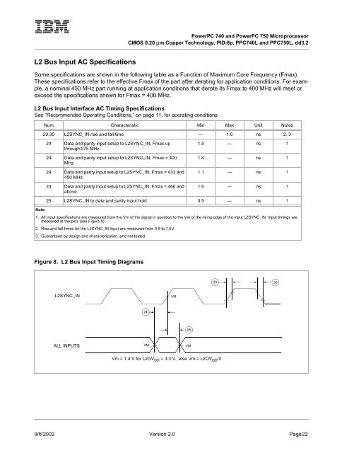
<strong>PowerPC</strong> <strong>740</strong> <strong>and</strong> <strong>PowerPC</strong> <strong>750</strong> <strong>Microprocessor</strong>CMOS 0.20 µm Copper Technology, PID-8p, PPC<strong>740</strong>L <strong>and</strong> PPC<strong>750</strong>L, dd3.2L2 Bus Input AC SpecificationsSome specifications are shown in the following table as a Function of Maximum Core Frequency (Fmax).These specifications refer to the effective Fmax of the part after derating for application conditions. For example,a nominal 450 MHz part running at application conditions that derate its Fmax to 400 MHz will meet orexceed the specifications shown for Fmax = 400 MHz.L2 Bus Input Interface AC Timing SpecificationsSee ”Recommended Operating Conditions,” on page 11, for operating conditions.Num Characteristic Min Max Unit Notes29,30 L2SYNC_IN rise <strong>and</strong> fall time — 1.0 ns 2, 324 Data <strong>and</strong> parity input setup to L2SYNC_IN, Fmax upthrough 375 MHz.24 Data <strong>and</strong> parity input setup to L2SYNC_IN, Fmax = 400MHz.24 Data <strong>and</strong> parity input setup to L2SYNC_IN, Fmax = 433 <strong>and</strong>450 MHz.24 Data <strong>and</strong> parity input setup to L2SYNC_IN, Fmax = 466 <strong>and</strong>above.1.5 — ns 11.4 — ns 11.1 — ns 11.0 — ns 125 L2SYNC_IN to data <strong>and</strong> parity input hold 0.5 — ns 1Note:1. All input specifications are measured from the Vm of the signal in question to the Vm of the rising edge of the input L2SYNC_IN. Input timings aremeasured at the pins (see Figure 8).2. Rise <strong>and</strong> fall times for the L2SYNC_IN input are measured from 0.5 to 1.5V.3. Guaranteed by design <strong>and</strong> characterization, <strong>and</strong> not tested.Figure 8. L2 Bus Input Timing Diagrams29 30L2SYNC_INVM2425ALL INPUTSVMVMVm = 1.4 V for L2OV DD = 3.3 V., else Vm = L2OV DD /29/6/2002 Version 2.0 Page 22


