

PowerPC 740 and PowerPC 750 Microprocessor Datasheet - IBM
PowerPC 740 and PowerPC 750 Microprocessor Datasheet - IBM
PowerPC 740 and PowerPC 750 Microprocessor Datasheet - IBM
- No tags were found...

Create successful ePaper yourself
Turn your PDF publications into a flip-book with our unique Google optimized e-Paper software.
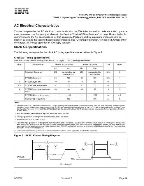
<strong>PowerPC</strong> <strong>740</strong> <strong>and</strong> <strong>PowerPC</strong> <strong>750</strong> <strong>Microprocessor</strong>CMOS 0.20 µm Copper Technology, PID-8p, PPC<strong>740</strong>L <strong>and</strong> PPC<strong>750</strong>L, dd3.2AC Electrical CharacteristicsThis section provides the AC electrical characteristics for the <strong>750</strong>. After fabrication, parts are sorted by maximumprocessor core frequency as shown in the Section “Clock AC Specifications,” on page 14, <strong>and</strong> tested forconformance to the AC specifications for that frequency. Parts are sold by maximum processor core frequency,subject to the specified application conditions. See ”Ordering Information,” on page 51. Unless otherwisenoted, all timings apply for all I/O supply voltages.Clock AC SpecificationsThe following table provides the clock AC timing specifications as defined in Figure 2.Clock AC Timing SpecificationsSee ”Recommended Operating Conditions,” on page 11, for operating conditions.Num Characteristic Fmax = 300-375MHz Fmax ≥ 400MHz Unit NotesMin Max Min MaxProcessor frequency 250 As specified bypart number250 As specified bypart numberMHz 6SYSCLK frequency 25 100 31 100 MHz 11 SYSCLK cycle time 10 40 10 32 ns2, 3 SYSCLK rise <strong>and</strong> fall time – 1.0 – 1.0 ns 2, 34 SYSCLK duty cycle measuredat Vm40 60 40 60 % 3SYSCLK jitter, cycle-to-cycle – ±150 – ±150 ps 4, 3Internal PLL relock time – 100 – 100 µs 5Note:1. Caution: The SYSCLK frequency <strong>and</strong> the PLL_CFG[0:3] settings must be chosen such that the resulting SYSCLK (bus) frequency, <strong>and</strong> CPU (core)frequency do not exceed their respective maximum or minimum operating frequencies. Refer to the PLL_CFG[0:3] signal description in Section “PLLConfiguration,” on page 40 for valid PLL_CFG[0:3] settings. Bus operation above 100 MHz is possible, but requires careful timing analysis. Contact<strong>IBM</strong> for details.2. Rise <strong>and</strong> fall times for the SYSCLK input are measured from 0.5 to 1.5V.3. Timing is guaranteed by design <strong>and</strong> characterization, <strong>and</strong> is not tested.4. Short term jitter must be under ±150ps.5. Relock timing is guaranteed by design <strong>and</strong> characterization, <strong>and</strong> is not tested. PLL-relock time is the maximum amount of time required for PLL lockafter a stable V DD <strong>and</strong> SYSCLK are reached during the power-on reset sequence. This specification also applies when the PLL has been disabled <strong>and</strong>subsequently re-enabled during sleep mode. Also note that HRESET must be held asserted for a minimum of 255 bus clocks after the PLL-relock timeduring the power-on reset sequence.6. Under certain conditions, operation at core frequencies below those stated is possible. Contact <strong>IBM</strong> for details.Figure 2. SYSCLK Input Timing Diagram41423CV IHSYSCLKVMCV ILVm = OV DD /29/6/2002 Version 2.0 Page 14


