Power Optimization and Prediction Techniques for FPGAs - Jason H ...
Power Optimization and Prediction Techniques for FPGAs - Jason H ...
Power Optimization and Prediction Techniques for FPGAs - Jason H ...

Create successful ePaper yourself
Turn your PDF publications into a flip-book with our unique Google optimized e-Paper software.
AcknowledgmentsThroughout my life, I have had great teachers <strong>and</strong> mentors. First, thank you to my advisor,Professor Farid Najm, <strong>for</strong> his guidance throughout my doctoral studies. He helped to set thedirection <strong>for</strong> this research by encouraging me to pursue paths that initially were unfamiliarto me. His steady, solid, <strong>and</strong> rigorous approach to research is something I aim to practicein my own career. Many thanks to Professors Zhu, Rose, Chow, Sheikholeslami, <strong>and</strong> Tessier<strong>for</strong> reviewing <strong>and</strong> evaluating this work. I also acknowledge Profs. Brown <strong>and</strong> Rose <strong>for</strong> thesignificant <strong>and</strong> lasting roles they played in early stages of my research career.I am indebted to my mentors at Xilinx, who, during my four years in San Jose, helped meto develop professional <strong>and</strong> technical skills that enabled me to produce <strong>and</strong> succeed in graduateschool. Thanks Rajeev, Sudip, Jim, <strong>and</strong> S<strong>and</strong>or! Thanks also to the members of the Xilinxplace <strong>and</strong> route team who seamlessly accepted a remote, part-time guy in Toronto. I am gratefulto Xilinx <strong>for</strong> giving me the opportunity to continue to work part-time during my PhD studies,<strong>and</strong> <strong>for</strong> allowing us to demonstrate a portion of this work using Xilinx technology. Thanksto Tim Tuan of Xilinx Research Labs <strong>for</strong> being a great sounding board, <strong>and</strong> <strong>for</strong> his technicalassistance. To all of my friends within Xilinx: thanks <strong>for</strong> the welcome diversions throughoutmy PhD.I have thoroughly enjoyed being in graduate school <strong>and</strong> it’s not an experience I would trade<strong>for</strong> any other. Many thanks go to my fellow graduate students in the Computer Group <strong>and</strong>especially, my office mates in LP392, both current <strong>and</strong> <strong>for</strong>mer, in particular: Imad, Navid, Denis,Lesley, Andy, Paul, Tom, Peter, Anish, Ian, Aaron, Mehrdad, Vince, <strong>and</strong> Warren. Thanks toKelly Chan <strong>for</strong> the dependable <strong>and</strong> conscientious administrative support.I wish to express my appreciation to the Natural Sciences <strong>and</strong> Engineering Research Council(NSERC) of Canada <strong>for</strong> the PGS scholarship, <strong>and</strong> to the Government of Ontario <strong>for</strong> the OGS<strong>and</strong> OGS-ST scholarships.Finally, thank you to my wife, Mary, <strong>for</strong> her love <strong>and</strong> support throughout our 8 yearstogether, <strong>and</strong> <strong>for</strong> always encouraging me to do whatever I enjoy.v
Acknowledgementsvi
ContentsAcknowledgmentsList of FiguresList of Tablesvxixv1 Introduction 11.1 Field-Programmable Gate Arrays . . . . . . . . . . . . . . . . . . . . . . . . . . . 11.2 Motivation . . . . . . . . . . . . . . . . . . . . . . . . . . . . . . . . . . . . . . . 21.3 Thesis Contributions . . . . . . . . . . . . . . . . . . . . . . . . . . . . . . . . . . 41.4 Thesis Organization . . . . . . . . . . . . . . . . . . . . . . . . . . . . . . . . . . 72 Background <strong>and</strong> Related Work 92.1 Introduction . . . . . . . . . . . . . . . . . . . . . . . . . . . . . . . . . . . . . . . 92.2 <strong>Power</strong> Dissipation in CMOS Circuits . . . . . . . . . . . . . . . . . . . . . . . . . 92.2.1 Dynamic <strong>Power</strong> . . . . . . . . . . . . . . . . . . . . . . . . . . . . . . . . . 92.2.2 Static (Leakage) <strong>Power</strong> . . . . . . . . . . . . . . . . . . . . . . . . . . . . 122.3 FPGA Architecture <strong>and</strong> Hardware Structures . . . . . . . . . . . . . . . . . . . . 202.4 <strong>Power</strong> Dissipation in <strong>FPGAs</strong> . . . . . . . . . . . . . . . . . . . . . . . . . . . . . 262.4.1 Dynamic <strong>Power</strong> . . . . . . . . . . . . . . . . . . . . . . . . . . . . . . . . . 262.4.2 Static (Leakage) <strong>Power</strong> . . . . . . . . . . . . . . . . . . . . . . . . . . . . 262.5 FPGA <strong>Power</strong> <strong>Optimization</strong> . . . . . . . . . . . . . . . . . . . . . . . . . . . . . . 282.5.1 Leakage <strong>Power</strong> <strong>Optimization</strong> . . . . . . . . . . . . . . . . . . . . . . . . . 282.5.2 Dynamic <strong>Power</strong> <strong>Optimization</strong> (Architecture/Circuit <strong>Techniques</strong>) . . . . . 292.5.3 Dynamic <strong>Power</strong> <strong>Optimization</strong> (CAD <strong>Techniques</strong>) . . . . . . . . . . . . . . 332.6 Summary . . . . . . . . . . . . . . . . . . . . . . . . . . . . . . . . . . . . . . . . 38vii
Contents3 CAD <strong>Techniques</strong> <strong>for</strong> Leakage <strong>Optimization</strong> 393.1 Introduction . . . . . . . . . . . . . . . . . . . . . . . . . . . . . . . . . . . . . . . 393.2 FPGA Hardware Structures . . . . . . . . . . . . . . . . . . . . . . . . . . . . . . 403.3 Active Leakage <strong>Power</strong> <strong>Optimization</strong> via Polarity Selection . . . . . . . . . . . . . 453.3.1 Experimental Study <strong>and</strong> Results . . . . . . . . . . . . . . . . . . . . . . . 513.4 Active Leakage <strong>Power</strong> <strong>Optimization</strong> via Leakage-Aware Routing . . . . . . . . . 633.4.1 Experimental Study <strong>and</strong> Results . . . . . . . . . . . . . . . . . . . . . . . 653.5 Summary . . . . . . . . . . . . . . . . . . . . . . . . . . . . . . . . . . . . . . . . 694 Circuit <strong>Techniques</strong> <strong>for</strong> Low-<strong>Power</strong> Interconnect 714.1 Introduction . . . . . . . . . . . . . . . . . . . . . . . . . . . . . . . . . . . . . . . 714.2 Preliminaries . . . . . . . . . . . . . . . . . . . . . . . . . . . . . . . . . . . . . . 724.2.1 Related Work . . . . . . . . . . . . . . . . . . . . . . . . . . . . . . . . . . 724.2.2 FPGA Interconnect Structures . . . . . . . . . . . . . . . . . . . . . . . . 734.3 Low-<strong>Power</strong> Routing Switch Design . . . . . . . . . . . . . . . . . . . . . . . . . . 744.4 Slack Analysis . . . . . . . . . . . . . . . . . . . . . . . . . . . . . . . . . . . . . . 814.5 Experimental Study . . . . . . . . . . . . . . . . . . . . . . . . . . . . . . . . . . 824.5.1 Methodology . . . . . . . . . . . . . . . . . . . . . . . . . . . . . . . . . . 824.5.2 Leakage <strong>Power</strong> Results . . . . . . . . . . . . . . . . . . . . . . . . . . . . . 854.5.3 Dynamic <strong>Power</strong> Results . . . . . . . . . . . . . . . . . . . . . . . . . . . . 924.5.4 Summary of Results . . . . . . . . . . . . . . . . . . . . . . . . . . . . . . 944.6 Summary . . . . . . . . . . . . . . . . . . . . . . . . . . . . . . . . . . . . . . . . 965 <strong>Power</strong>-Aware Technology Mapping 995.1 Introduction . . . . . . . . . . . . . . . . . . . . . . . . . . . . . . . . . . . . . . . 995.2 Preliminaries . . . . . . . . . . . . . . . . . . . . . . . . . . . . . . . . . . . . . . 1005.2.1 <strong>Power</strong> <strong>and</strong> Logic Replication . . . . . . . . . . . . . . . . . . . . . . . . . 1015.3 Algorithm Description . . . . . . . . . . . . . . . . . . . . . . . . . . . . . . . . . 1045.3.1 Generating K-Feasible Cuts . . . . . . . . . . . . . . . . . . . . . . . . . . 1045.3.2 Costing Cuts . . . . . . . . . . . . . . . . . . . . . . . . . . . . . . . . . . 1065.3.3 Mapping . . . . . . . . . . . . . . . . . . . . . . . . . . . . . . . . . . . . . 1105.4 Experimental Study <strong>and</strong> Results . . . . . . . . . . . . . . . . . . . . . . . . . . . 1105.4.1 Methodology . . . . . . . . . . . . . . . . . . . . . . . . . . . . . . . . . . 1105.4.2 Results . . . . . . . . . . . . . . . . . . . . . . . . . . . . . . . . . . . . . 1135.5 Impact of Research . . . . . . . . . . . . . . . . . . . . . . . . . . . . . . . . . . . 118viii
Contentsx
List of Figures2.1 Equivalent circuit <strong>for</strong> a CMOS gate charging <strong>and</strong> discharging a capacitor [Yeap 98]. 102.2 Leakage mechanisms in an NMOS transistor. . . . . . . . . . . . . . . . . . . . . 132.3 Gate oxide leakage dependence on oxide thickness <strong>and</strong> gate bias [Thom 98]. . . . 152.4 Scaling of gate length <strong>and</strong> supply voltage [Doyl 02]. . . . . . . . . . . . . . . . . . 162.5 Scaling of V DD , V T H , <strong>and</strong> t ox with process generation [Taur 02]. . . . . . . . . . . 172.6 Scaling of subthreshold leakage power density <strong>and</strong> dynamic power density [Nowa 02]. 182.7 ASIC leakage optimization techniques. . . . . . . . . . . . . . . . . . . . . . . . . 202.8 (a) Abstract FPGA architecture; (b) logic block; (c) LUT. . . . . . . . . . . . . . 212.9 Logic blocks in Xilinx <strong>and</strong> Altera commercial <strong>FPGAs</strong>. . . . . . . . . . . . . . . . 232.10 FPGA routing switch. . . . . . . . . . . . . . . . . . . . . . . . . . . . . . . . . . 242.11 Multiplexers as deployed in FPGA routing switches <strong>and</strong> a LUT. . . . . . . . . . 252.12 Dynamic power breakdown in Xilinx Virtex-II [Shan 02]. . . . . . . . . . . . . . . 272.13 Leakage power breakdown in Xilinx Spartan-3 [Tuan 03]. . . . . . . . . . . . . . 282.14 Multiplexer leakage reduction techniques [Rahm 04]. . . . . . . . . . . . . . . . . 302.15 Dual-V DD FPGA structures. . . . . . . . . . . . . . . . . . . . . . . . . . . . . . 322.16 Typical FPGA CAD flow. . . . . . . . . . . . . . . . . . . . . . . . . . . . . . . . 342.17 <strong>Power</strong>-aware technology mapping. . . . . . . . . . . . . . . . . . . . . . . . . . . 352.18 Basis of post-layout power optimization. . . . . . . . . . . . . . . . . . . . . . . . 373.1 Two 4-to-1 multiplexer implementations. . . . . . . . . . . . . . . . . . . . . . . . 403.2 Leakage power <strong>for</strong> multiplexers. . . . . . . . . . . . . . . . . . . . . . . . . . . . . 423.3 Examples of transistor leakage states. . . . . . . . . . . . . . . . . . . . . . . . . 433.4 Buffer implementation <strong>and</strong> leakage power. . . . . . . . . . . . . . . . . . . . . . . 443.5 Low temperature leakage power results <strong>for</strong> multiplexers <strong>and</strong> buffer (40 ◦ C). . . . . 463.6 LUT circuit implementation; illustration of signal inversion. . . . . . . . . . . . . 473.7 Leakage optimization algorithm. . . . . . . . . . . . . . . . . . . . . . . . . . . . 483.8 Static probability versus switching activity. . . . . . . . . . . . . . . . . . . . . . 51xi
List of Figures6.4 Finding the set of path lengths <strong>for</strong> y. . . . . . . . . . . . . . . . . . . . . . . . . . 1326.5 Zero-delay activity <strong>and</strong> predicted activity versus routed-delay activity. . . . . . . 1366.6 Logic-delay activity <strong>and</strong> predicted activity versus routed-delay activity. . . . . . 1376.7 Noise in interconnect capacitance. . . . . . . . . . . . . . . . . . . . . . . . . . . 1426.8 Illustration of parameter NT . . . . . . . . . . . . . . . . . . . . . . . . . . . . . . 1446.9 Routing congestion estimation. . . . . . . . . . . . . . . . . . . . . . . . . . . . . 1466.10 Average error <strong>for</strong> a variety of prediction models. . . . . . . . . . . . . . . . . . . 1486.11 Estimated versus actual values (approx. 4000 points in ellipse). . . . . . . . . . . 150xiii
List of Figuresxiv
List of Tables2.1 Summary of commercial FPGA routing architectures (lengths given in CLB tilesor LAB tiles, as appropriate). . . . . . . . . . . . . . . . . . . . . . . . . . . . . . 243.1 Major circuit blocks in target FPGA. . . . . . . . . . . . . . . . . . . . . . . . . . 523.2 Characteristics of benchmark circuits. . . . . . . . . . . . . . . . . . . . . . . . . 543.3 Detailed active leakage power results. . . . . . . . . . . . . . . . . . . . . . . . . . 603.4 Effect of leakage-aware routing on critical path delay. . . . . . . . . . . . . . . . . 663.5 Detailed active leakage power results <strong>for</strong> leakage-aware routing combined withpolarity selection. . . . . . . . . . . . . . . . . . . . . . . . . . . . . . . . . . . . . 684.1 85 ◦ C leakage power reduction results <strong>for</strong> basic design (unshaded) <strong>and</strong> alternatedesign (shaded). . . . . . . . . . . . . . . . . . . . . . . . . . . . . . . . . . . . . 894.2 25 ◦ C leakage power reduction results <strong>for</strong> basic design (unshaded) <strong>and</strong> alternatedesign (shaded). . . . . . . . . . . . . . . . . . . . . . . . . . . . . . . . . . . . . 904.3 85 ◦ C leakage power reduction results <strong>for</strong> basic+MUX design (unshaded) <strong>and</strong>alternate+MUX design (shaded). . . . . . . . . . . . . . . . . . . . . . . . . . . . 914.4 25 ◦ C leakage power reduction results <strong>for</strong> basic+MUX design (unshaded) <strong>and</strong>alternate+MUX design (shaded). . . . . . . . . . . . . . . . . . . . . . . . . . . . 914.5 Sleep mode leakage results 85 ◦ C (unshaded) <strong>and</strong> 25 ◦ C (shaded). . . . . . . . . . 924.6 Dynamic power results <strong>for</strong> all switch designs. . . . . . . . . . . . . . . . . . . . . 935.1 Detailed results <strong>for</strong> depth-optimal 4-LUT mapping solutions. . . . . . . . . . . . 1156.1 Characteristics of benchmark circuits. . . . . . . . . . . . . . . . . . . . . . . . . 1256.2 Effect of glitching on switching activity. . . . . . . . . . . . . . . . . . . . . . . . 1276.3 Error in predicted activity values. . . . . . . . . . . . . . . . . . . . . . . . . . . . 1356.4 Error in predicted activity values <strong>for</strong> alternate benchmark division. . . . . . . . . 1396.5 Noise in individual circuits. . . . . . . . . . . . . . . . . . . . . . . . . . . . . . . 142xv
List of Tables6.6 Errors <strong>for</strong> individual circuits; results <strong>for</strong> alternate characterization/test benchmarkdivision). . . . . . . . . . . . . . . . . . . . . . . . . . . . . . . . . . . . . . 150A.1 <strong>Prediction</strong> model <strong>and</strong> regression analysis details (zero-delay activity <strong>and</strong> logicdelayactivity-based prediction models). . . . . . . . . . . . . . . . . . . . . . . . 160A.2 <strong>Prediction</strong> model <strong>and</strong> regression analysis details (low-fanout <strong>and</strong> high-fanoutprediction models). . . . . . . . . . . . . . . . . . . . . . . . . . . . . . . . . . . . 161xvi
1 Introduction1.1 Field-Programmable Gate ArraysField-programmable gate arrays (<strong>FPGAs</strong>) are programmable logic devices (PLDs) that can beconfigured by the end-user to implement virtually any digital circuit. Since first introducedin the mid-80s, the popularity of <strong>FPGAs</strong> has grown steadily, <strong>and</strong> today, <strong>FPGAs</strong> account <strong>for</strong>more than half of the 3 billion dollar programmable logic industry. State-of-the-art <strong>FPGAs</strong> canimplement circuits with millions of gates that operate at speeds in the hundreds of megahertz.The focus of this dissertation is the optimization <strong>and</strong> prediction of power consumption in<strong>FPGAs</strong>, through novel computer-aided design (CAD) algorithms, as well as circuit-level designtechniques.An FPGA is a VLSI chip consisting of a pre-fabricated two-dimensional array of programmablelogic blocks that connect to one another through a configurable interconnection(routing) network. Static RAM (SRAM) cells, internal to the FPGA, define the logic functionimplemented by each logic block <strong>and</strong> the desired connectivity between logic blocks. AnFPGA can be configured to implement a given circuit in a matter of seconds <strong>and</strong> can be reprogrammedany number of times. Custom ASICs are the primary competitor to <strong>FPGAs</strong>, <strong>and</strong>they require weeks or months <strong>for</strong> fabrication. Hence, a key advantage held by <strong>FPGAs</strong> overASICs is that <strong>FPGAs</strong> reduce “time-to-market”, which is crucial in the development of newelectronic products.The rapid expansion of the programmable logic market has been driven by a number offactors. Perhaps most important is that as technology scales, the costs associated with buildinga custom ASIC rise drastically. For example, in 90nm process technology, the cost of mask sets1
1 Introductionalone is over a million US dollars [Lamm 03]. Such costs make design mistakes extremely costly,as they necessitate the creation of new mask sets <strong>and</strong> impose lengthy delays. Comprehensive<strong>and</strong> rigorous design verification is a m<strong>and</strong>atory part of custom ASIC design. In <strong>FPGAs</strong>, therequirement to “get it right the first time” is less critical, since mistakes, once identified, canbe taken care of quickly <strong>and</strong> cheaply by re-programming the device.Coupled with the high cost of ASIC fabrication, the CAD tools required to design an ASICcost anywhere from hundreds of thous<strong>and</strong>s to millions of dollars [Sant 03]. In contrast, FPGAvendor tools are typically provided free-of-charge by the FPGA vendors to their best customers,<strong>and</strong> third-party FPGA CAD tools, such as Synplicity, cost only tens of thous<strong>and</strong>s of dollars.Initially, <strong>FPGAs</strong> were used only in low-volume production applications or <strong>for</strong> prototyping circuitsthat were eventually to be implemented as custom ASICs. However, the volume thresholdat which <strong>FPGAs</strong> are cost-effective versus ASICs has advanced to a point such that modern<strong>FPGAs</strong> are cost-effective <strong>for</strong> all but high volume applications.One of the drawbacks of <strong>FPGAs</strong> is that they are less area-efficient <strong>and</strong> also slower thancustom ASICs. This characteristic has been the motivation <strong>for</strong> nearly two decades of academic<strong>and</strong> industrial research on FPGA CAD <strong>and</strong> architecture. The result has been a narrowing ofthe “gap” between ASICs <strong>and</strong> <strong>FPGAs</strong> from the area <strong>and</strong> speed viewpoints. Today, <strong>FPGAs</strong>are a viable alternative to custom ASICs <strong>and</strong> can be used in applications with speed <strong>and</strong> sizerequirements that previously, could only be met by ASICs.1.2 MotivationThe ability to program <strong>and</strong> re-program an FPGA involves significant hardware overhead. Moretransistors are needed to implement a given logic circuit in an FPGA in comparison with acustom ASIC. This leads to a higher power consumption per logic gate in <strong>FPGAs</strong> [Geor 01,Zuch 02], <strong>and</strong> power-efficiency is undisputed as an area in which ASICs are superior to FP-GAs [Full 04]. In fact, power has been cited as a limiting factor in the ability of <strong>FPGAs</strong> tocontinue to replace ASICs [Stok 03].2
1.2 MotivationDespite the relative weakness of <strong>FPGAs</strong> from the power angle, their power consumption has,until recently, been largely ignored by the research community. Likewise, no commercial FPGAvendors offer hardware or software specifically targeted to low-power applications. The extentto which FPGA power can be optimized through either CAD, architecture, or circuit techniqueshas been an open question. The focus of commercial vendors, as well as the majority ofpublished research on FPGA architecture <strong>and</strong> CAD, has concentrated on improving FPGA areaefficiency<strong>and</strong> per<strong>for</strong>mance. A thorough treatment of prior research on FPGA speed <strong>and</strong> areais outside the scope here; however, references [Rose 89, Rose 91, Betz 96, Betz 97a, Betz 99a]present the first <strong>and</strong> seminal work on FPGA logic <strong>and</strong> routing architecture, with importantfollow-up work appearing in [Sing 90, Marq 99, Ahme 02]. CAD algorithms that optimize thearea <strong>and</strong> per<strong>for</strong>mance of <strong>FPGAs</strong> are well-studied, with some of the most important papers being[Brow 90, Fran 90, Fran 91a, Lemi 93, Cong 94a, Cong 94b, McMu 95, Betz 97b]. Thougharea <strong>and</strong> speed have been the main research focus to date, power is likely to be a key considerationin the design of future <strong>FPGAs</strong>, <strong>for</strong> the reasons outlined below.A well-known consequence of technology scaling is the rapid increase in static (leakage)power relative to dynamic power. Dynamic power is consumed as a result of logic transitionsthat occur on a circuit’s signals during normal operation. It increases in proportion to therate of logic transitions (switching activity) on circuit signals <strong>and</strong> the amount of capacitancecharged <strong>and</strong> discharged during logic transitions. Leakage power is consumed when a circuit is ina quiescent, idle state. Both dynamic <strong>and</strong> leakage power consumption have become major issues<strong>for</strong> semiconductor vendors <strong>and</strong> their customers [Inte 02]. Moreover, the considerable increase inleakage with each process generation has significant implications <strong>for</strong> <strong>FPGAs</strong>. Leakage currentin a circuit is proportional to the circuit’s total drawn transistor width [Jian 02]. Since <strong>FPGAs</strong>contain a huge number of transistors, as required to provide programmability, the need <strong>for</strong>effective leakage management techniques is amplified in <strong>FPGAs</strong> versus in other technologies.Given this, low leakage is certain to be a significant design objective in next-generation <strong>FPGAs</strong>.Optimizing the power consumption of <strong>FPGAs</strong> has a number of benefits.First, reduced3
1 Introductionpower is m<strong>and</strong>atory if <strong>FPGAs</strong> are to break into the low-power ASIC market. Historically,applications such as portable or battery-powered electronics have been inaccessible to FPGAvendors, chiefly due to the tight power budgets they impose. For example, mobile applicationshave st<strong>and</strong>by current limits of 10s to 100s of µA [Clar 02]. As few as 20 logic blocks in the XilinxSpartan-3 FPGA would exceed this st<strong>and</strong>by current limit [Tuan 03]. In addition to broadeningthe FPGA market, lowering power consumption would reduce packaging <strong>and</strong> cooling costs,which represent a sizable fraction of the cost of an IC. Packaging costs <strong>for</strong> a 90nm design arepotentially on par with the cost of the silicon itself [Hawk 03]. Finally, it is worth noting thatcooler chips have better reliability, leading to long lifespans.In conjunction with reducing FPGA power, as power becomes a first-class design consideration<strong>for</strong> <strong>FPGAs</strong>, efficient power-aware design will require new estimation tools that gauge powerdissipation at the early stages of the design process. Such tools would allow design trade-offsto be considered at a high level of abstraction, reducing design ef<strong>for</strong>t <strong>and</strong> cost.1.3 Thesis ContributionsThis dissertation focuses on two overarching themes:1. Reducing FPGA power consumption, including dynamic <strong>and</strong> static power.2. Early prediction of dynamic power consumption in <strong>FPGAs</strong>.With respect to these themes, a number of different contributions are made, as summarizedbelow.Chapter 3 considers active leakage power dissipation in <strong>FPGAs</strong> <strong>and</strong> presents two “no cost” approaches<strong>for</strong> active leakage reduction 1 . It is well-known that the leakage power consumedby a digital CMOS circuit depends strongly on the state of its inputs. The first leakagereduction technique leverages a fundamental property of basic FPGA logic elements1 Active leakage is leakage in the used <strong>and</strong> operating part of an FPGA.4
1.3 Thesis Contributions(look-up-tables) that allows a logic signal in an FPGA design to be interchanged with itscomplemented <strong>for</strong>m without any area or delay penalty. This property is applied to selectpolarities <strong>for</strong> logic signals so that FPGA hardware structures spend the majority of timein low leakage states. The second approach to leakage optimization consists of alteringthe routing step of the FPGA CAD flow to encourage more frequent use of routing resourcesthat have low leakage power consumptions. Such “leakage-aware routing” allowsactive leakage to be further reduced, without compromising design per<strong>for</strong>mance. In anexperimental study, active leakage power is optimized in circuits mapped into a stateof-the-art90nm commercial FPGA. Combined, the two approaches offer a total activeleakage power reduction of 30%, on average. This work has been published in [Ande 04f]<strong>and</strong> [Ande 05a]. To the author’s knowledge, this represents the first published work onactive leakage optimization in <strong>FPGAs</strong>.Chapter 4 presents circuit-level techniques <strong>for</strong> reducing power dissipation in FPGA interconnect.It proposes a family of new FPGA routing switch designs that are programmableto operate in three different modes: high-speed, low-power, or sleep. High-speed modeprovides similar power <strong>and</strong> per<strong>for</strong>mance to traditional FPGA routing switches. In lowpowermode, speed is curtailed in order to reduce power consumption. Leakage is reducedby 28-52% in low-power versus high-speed mode, depending on the particular switch designselected. Dynamic power is reduced by 28-31% in low-power mode. Leakage powerin sleep mode, which is suitable <strong>for</strong> unused routing switches, is 61-79% lower than inhigh-speed mode. Each of the proposed switch designs has a different power/area/speedtrade-off. All of the designs require only minor changes to a traditional routing switch,making them easy to incorporate into current FPGA interconnect. The applicability ofthe new switches is motivated through an analysis of timing slack in industrial FPGA designs.Specifically, it is observed that a considerable fraction of routing switches may beslowed down (operate in low-power mode), without impacting overall design per<strong>for</strong>mance.This work has been published in [Ande 04c], [Ande 04d], <strong>and</strong> [Ande 05b].5
1 IntroductionChapter 5 presents a new power-aware technology mapping algorithm <strong>for</strong> look-up-table-based<strong>FPGAs</strong>. The algorithm aims to keep nets with high switching activity out of the FPGArouting network, <strong>and</strong> takes an activity-conscious approach to logic replication. Logicreplication is known to be crucial <strong>for</strong> optimizing depth in technology mapping. An importantcontribution of this work is to recognize the effect of logic replication on circuitstructure <strong>and</strong> to show its consequences on power. In an experimental study, the powercharacteristics of mapping solutions generated by several publicly available technologymappers are examined. Results show that <strong>for</strong> a specific depth of mapping solution, thepower consumption can vary considerably, depending on the technology mapping approachused. Furthermore, results show that the proposed mapping algorithm leads tocircuits with substantially less power dissipation than mappings produced by previousapproaches. This work has been published in [Ande 02]. To the author’s knowledge, thisrepresents the first work on power/depth trade-offs in FPGA technology mapping.Chapter 6 explores early power prediction <strong>for</strong> <strong>FPGAs</strong>. As mentioned above, the dynamicpower consumed by a digital CMOS circuit is directly proportional to both switchingactivity <strong>and</strong> interconnect capacitance. Chapter 6 considers early prediction of activity<strong>and</strong> capacitance in FPGA designs. Empirical prediction models are developed <strong>for</strong> theseparameters, suitable <strong>for</strong> use in power-aware layout synthesis, early power planning, <strong>and</strong>other applications. The models can be applied early in the design process, when detailedrouting data is incomplete or unavailable. The impact of delay on switching activity in<strong>FPGAs</strong> is studied by examining how the switching activity of a signal changes when delaysare zero (zero-delay activity) versus when logic delays are considered (logic-delay activity)versus when both logic <strong>and</strong> routing delays are considered (routed-delay activity). A novelapproach <strong>for</strong> pre-layout activity prediction is proposed that estimates a signal’s routeddelayactivity using only zero-delay or logic-delay activity values, along with structural <strong>and</strong>functional circuit properties. For capacitance prediction, the model’s prediction accuracyis improved by considering aspects of the FPGA interconnect architecture in addition6
1.4 Thesis Organizationto generic parameters, such as signal fanout <strong>and</strong> bounding box perimeter length. Wealso demonstrate that there is an inherent variability (noise) in switching activity <strong>and</strong>capacitance that limits the accuracy attainable in prediction. Experimental results showthat the proposed prediction models work well given the noise limitations. This work hasbeen published in [Ande 03], [Ande 04b], <strong>and</strong> [Ande 04e].1.4 Thesis OrganizationThe remainder of this dissertation is organized as follows: Chapter 2 reviews the backgroundmaterial relevant to the research, including a description of static <strong>and</strong> dynamic power consumptionin CMOS circuits, the impact of technology scaling on leakage, an overview of FPGAtechnology, <strong>and</strong> coverage of recent research on FPGA power optimization.The main research contributions, highlighted above, are presented in Chapters 3, 4, 5, <strong>and</strong> 6.For clarity, <strong>and</strong> owing to the range of topics considered, each chapter is self-contained. Thatis, the experimental results <strong>for</strong> each proposed power optimization or prediction technique arepresented together with the technique’s description in a single chapter.Chapter 7 presents concluding remarks <strong>and</strong> suggestions <strong>for</strong> future work.7
1 Introduction8
2 Background <strong>and</strong> Related Work2.1 IntroductionThis chapter presents the background material that <strong>for</strong>ms the basis <strong>for</strong> the research presented inlater chapters. Section 2.2 reviews power dissipation in CMOS circuits, covering both dynamic,as well as static power. Section 2.3 gives an overview of FPGA architecture <strong>and</strong> hardwarestructures, highlighting the features of two state-of-the-art commercial <strong>FPGAs</strong>. Section 2.4examines power dissipation in the FPGA context <strong>and</strong> discusses the breakdown of dynamic <strong>and</strong>static power dissipation in <strong>FPGAs</strong>. Section 2.5 surveys the recent literature on FPGA poweroptimization.2.2 <strong>Power</strong> Dissipation in CMOS Circuits<strong>Power</strong> consumption in CMOS circuits can be classified as either dynamic or static. Dynamicpower consumption is due to the logic transitions that occur on the signals of a logic circuit.Such transitions occur as a normal part of useful computation, <strong>and</strong> dynamic power scales inproportion to the rate of computation. Static power, on the other h<strong>and</strong>, also referred to asleakage power, is dissipated when a logic circuit is in a quiescent state.2.2.1 Dynamic <strong>Power</strong>Dynamic power is consumed through two mechanisms: short-circuit current <strong>and</strong> the charging<strong>and</strong> discharging of capacitance [Yeap 98]. Short-circuit current arises in a CMOS gate as itsoutput transitions between logic states. During a transition, both the pull-up <strong>and</strong> pull-down9
2 Background <strong>and</strong> Related WorkFigure 2.1: Equivalent circuit <strong>for</strong> a CMOS gate charging <strong>and</strong> discharging a capacitor [Yeap 98].networks conduct concurrently <strong>for</strong> a short time window, resulting in a temporary short-circuitpath from supply to ground within the gate. In well-designed circuits, short-circuit currenttypically represents only 5-10% of dynamic power [Chan 92]. By far, the majority of dynamicpower dissipation is due to charging <strong>and</strong> discharging capacitance [Yeap 98].Figure 2.1 shows an equivalent circuit <strong>for</strong> a CMOS gate charging or discharging a capacitanceC, where V DD represents the voltage supply <strong>and</strong> R c (R d ) represents the resistance of thecharging (discharging) circuitry 1 . The time dependent current/voltage characteristics of thecapacitor are given by:i c (t) = C dv c(t)dt(2.1)Assume that the capacitor is initially uncharged at time t 0 <strong>and</strong> that it is fully charged at time t 1 ;that is, v c (t 0 ) = 0 <strong>and</strong> v c (t 1 ) = V DD . The total energy drawn from the supply to charge thecapacitor is given by:E s =∫ t1t 0V DD · i c (t) dt (2.2)1 Internal gate capacitances are ignored in the model of Figure 2.1.10
2.2 <strong>Power</strong> Dissipation in CMOS CircuitsSubstituting (2.1) into (2.2) yields:E s = C · V DD∫ t1t 0dv c (t)dt∫ VDD2dt = C · V DD dv c = C · V DD0(2.3)The energy drawn from the supply in a rising transition on the gate’s output signal, E 01 ,is equal to E s . No energy is drawn from the supply when discharging the capacitor in a fallingtransition, <strong>and</strong> there<strong>for</strong>e, E 10 = 0. The average energy consumed per transition on the gate’soutput signal is:E trans = E 01 + E 102= E s + 02= C · V DD 22(2.4)The average dynamic power consumed by the gate, P gate , depends on the average rate of logictransitions on gate’s output signal:P gate = F trans · E trans = F trans · C · V DD22(2.5)where F trans is referred to as the switching activity of the gate output signal <strong>and</strong> is expressed inunits of transitions per second. In clocked circuits, it is convenient to normalize the switchingactivity by the clock period as follows:F trans = F clk · F (2.6)where F clk represents the system clock frequency <strong>and</strong> F represents the average number oftransitions on the gate output signal per clock cycle. F is referred to as the normalized switchingactivity.Substituting (2.6) into (2.5) <strong>and</strong> summing over all signals yields the familiar equation <strong>for</strong>the average dynamic power consumed by a CMOS digital circuit:P avg = F clk2∑i ∈ signalsC(i) · F (i) · V DD2(2.7)where P avg represents average power consumption, C(i) is the load capacitance of a signal i,11
2 Background <strong>and</strong> Related Work<strong>and</strong> F (i) represents the average number of transitions on signal i per clock cycle (signal i’snormalized switching activity).Various approaches to computing switching activity have been proposed in the literature,<strong>and</strong> they can generally be classified as either simulation-based approaches or as probabilisticapproaches [Najm 94, Soel 00]. In a simulation-based approach, the circuit is simulatedwith representative vectors, <strong>and</strong> the simulation tool produces a profile of all signalactivities during the simulation. Probabilistic approaches <strong>for</strong> activity estimation are wellstudied(e.g., [Najm 93, Marc 98, Wrig 00, Chou 97, Juan 01, Meht 95]). These approachesrequire no simulation vectors. Rather, a user is simply required to specify the switching activity,<strong>and</strong> possibly other properties, of the circuit’s primary inputs. An algorithmic approach isused to compute activities <strong>for</strong> the circuit’s internal signals. The advantage of probabilistic approachesover simulation is primarily run-time; the disadvantage is that probabilistic approachesare generally less accurate.When delays are considered, switching activity normally increases due to the introductionof glitches, which are spurious logic transitions on a signal caused by unequal path delays tothe signal’s driving gate. As transitions on gate inputs occur at different times, the signalexperiences multiple transitions be<strong>for</strong>e settling to its final value. The extra activity due toglitching consumes dynamic power, <strong>and</strong> previous work has suggested that 20-70% of totalpower dissipation in ASICs can be due to glitches [Shen 92].Chapter 6 studies switching activity, glitching severity, <strong>and</strong> capacitance in <strong>FPGAs</strong> <strong>and</strong>presents new techniques <strong>for</strong> early dynamic power estimation.2.2.2 Static (Leakage) <strong>Power</strong>The primary leakage mechanisms in an MOS transistor are illustrated in Figure 2.2, <strong>and</strong> consistof subthreshold leakage, gate oxide leakage, <strong>and</strong> junction leakage (also called b<strong>and</strong>-to-b<strong>and</strong> tunnelingleakage) [Agar 04]. Junction leakage comprises a small fraction of total leakage [Doyl 02],<strong>and</strong> refers to the current flow across the reverse-biased p-n junctions at the interface between12
2.2 <strong>Power</strong> Dissipation in CMOS Circuitssourcegate oxideleakagegatedrainjunctionleakagen + n +subthreshold leakagejunctionleakagebody (bulk)Figure 2.2: Leakage mechanisms in an NMOS transistor.the source/drain <strong>and</strong> the substrate. The two dominant leakage mechanisms are subthresholdleakage <strong>and</strong> gate oxide leakage [Doyl 02, Nowa 02]. These two mechanisms, as well as the wayin which they are impacted by technology scaling, are described below.An “ideal” MOS transistor can be viewed as a perfect switch, with the gate terminal exhibitingperfect control over the drain-to-source current (I DS ). When the potential differencebetween the gate <strong>and</strong> source (V GS ) is less than the transistor’s threshold voltage (V T H ), thetransistor is said to be OFF <strong>and</strong> in the cut-off state. Ideally, I DS = 0 in cut-off. In realityhowever, a non-zero subthreshold current may flow between the drain <strong>and</strong> source terminals incut-off. Subthreshold leakage in a transistor depends on process parameters as well as biasconditions, as modeled by [Roy 03]:I DS = A × e qmkT (V GS−V T H )× (1 − e −V DS qkT ) (2.8)whereV T H = V th0 − γ′ · V S + η · V DS (2.9)<strong>and</strong>13
2 Background <strong>and</strong> Related WorkWA = µ 0 C ox ( kT L eff q )2 e 1.8 (2.10)The parameters in (2.8), (2.9), <strong>and</strong> (2.10) are defined as follows: V th0 is the zero-biasthreshold voltage, γ′ is the linearized body effect coefficient, η is called the drain-inducedbarrier lowering coefficient, C ox is the gate oxide capacitance, µ 0 is the zero-bias mobility, mis the subthreshold swing, W <strong>and</strong> L eff are the width <strong>and</strong> effective length of the transistor,k represents Boltzmann’s constant, T is temperature in degrees Kelvin, <strong>and</strong> q is the electroncharge.From (2.8), (2.9), <strong>and</strong> (2.10), several interesting properties of subthreshold leakage can beinferred. First, subthreshold leakage increases exponentially as threshold voltage is reduced<strong>and</strong> decreases exponentially as gate/source bias (V GS ) is reduced. These properties arise fromthe first exponential term of (2.8). Second, threshold voltage depends on the drain/source bias(V DS ). This is referred to as drain-induced barrier lowering (DIBL), <strong>and</strong> is modeled by thethird term on the right side of (2.9). Finally, subthreshold leakage increases exponentially withtemperature, roughly doubling <strong>for</strong> every 10 ◦ C increase in temperature [Nowa 02].Similar to how an MOS transistor is a non-ideal switch, the gate terminal of a transistor isan imperfect insulator. Gate oxide leakage is due to a non-zero tunneling current through theinsulating gate oxide. It increases exponentially as oxide thickness is reduced. It also increasesexponentially as the potential difference across the gate oxide is increased [Lee 04, Kris 02,Nowa 02]. Figure 2.3 (from [Thom 98]) illustrates the exponential dependence of gate oxideleakage on gate bias <strong>and</strong> oxide thickness. For an NMOS device, in the ON state, gate oxideleakage flows from the gate terminal to the channel, drain, source, <strong>and</strong> substrate [Agar 04], in amechanism referred to as direct tunneling [Roy 03]. In the OFF state, the overlap between thegate <strong>and</strong> the source/drain regions permits leakage from the source/drain to the gate terminal.This is referred to as edge-directed tunneling, <strong>and</strong> its magnitude is much smaller than directtunneling gate leakage [Lee 04].14
2.2 <strong>Power</strong> Dissipation in CMOS Circuits10 4I GATE(A/cm 2 )10 010 -80 1 2 3Gate voltage (V)Figure 2.3: Gate oxide leakage dependence on oxide thickness <strong>and</strong> gate bias [Thom 98].Impact of Technology Scaling on Leakage“The number of transistors on an integrated circuit doubles every 18 months.”Moore’s Law, first stated in the 1960s, has largely remained true <strong>for</strong> four decades, <strong>and</strong> isthe basis <strong>for</strong> the incredible growth of the semiconductor industry throughout this period. Suchdrastic scaling has been made possible by the seemingly endless ability to shrink the size of atransistor, markedly increasing the density of transistors on a single IC.As transistors are made smaller, there are two important consequences. First, the exponentialgrowth in the number of devices on a single chip leads to a higher power consumption.Second, the electric fields internal to a transistor increase, which impacts transistor reliability 2 .To address these issues, supply voltage must be scaled in t<strong>and</strong>em with feature size. Figure 2.4(from [Doyl 02]) shows the scaling of transistor gate length <strong>and</strong> supply voltage versus processgeneration. The supply voltage scales at approximately 0.85X per generation; the gate lengthscales at approximately 0.65X per generation.The drive capability <strong>and</strong> associated speed per<strong>for</strong>mance of a transistor depends on the mag-2 Field strength in an MOS transistor influences failure due to gate oxide breakdown [Amer 98].15
2 Background <strong>and</strong> Related Work100010.0Gate length (nm)1001.0Supply voltage (V)10750 350 180 95 45Process generation (nm)0.1Figure 2.4: Scaling of gate length <strong>and</strong> supply voltage [Doyl 02].nitude of V DD −V T H [Sedr 97]. Consequently, as supply voltages are reduced, threshold voltagesmust also be reduced to mitigate per<strong>for</strong>mance degradations. As discussed in Section 2.2.2, reducingV T H yields an exponential increase in subthreshold leakage. Thus, smaller feature sizesnecessitate lower supply voltages, which in turn necessitate lower threshold voltages, which areassociated with increased subthreshold leakage current. To be sure, subthreshold leakage ispredicted to increase by roughly 5X per process generation [Bork 99].Additionally, a transistor’s drive current depends linearly on its gate oxide capacitance, C ox ,defined as:C ox =εt ox(2.11)where ε is the permittivity of the gate insulator <strong>and</strong> t ox is the oxide thickness. Current drive isimproved by thinning the oxide (reducing t ox ), producing an exponential increase in gate oxideleakage 3 . Figure 2.5 (from [Taur 02]) illustrates the scaling of supply voltage, oxide thickness,<strong>and</strong> threshold voltage with process generation.The scaling trends outlined above imply that leakage power will constitute an increasinglydominant component of total power in future process technologies.A survey conducted by3 Thinner oxides are also required to maintain adequate gate control over the drain current as technologyscales [Fran 02].16
2.2 <strong>Power</strong> Dissipation in CMOS Circuits105<strong>Power</strong> supply <strong>and</strong> threshold voltage (V)210.50.20.1V DD1V THt ox5020105Gate oxide thickness (nm)20.02 0.05 0.1 0.2 0.5 1MOSFET channel length (microns)Figure 2.5: Scaling of V DD , V T H , <strong>and</strong> t ox with process generation [Taur 02].17
2 Background <strong>and</strong> Related Work100010010?Active-powerdensity<strong>Power</strong> (W/cm 2 )10.10.01Subthreshold-powerdensity0.0010.000125° C data10 -50.01 0.1 1Gate Length (um)Figure 2.6: Scaling of subthreshold leakage power density <strong>and</strong> dynamic power density [Nowa 02].Nowak produced the trend data shown in Figure 2.6 [Nowa 02]. The figure clearly illustratesthat both static <strong>and</strong> dynamic power increase as technology scales; however, the rate of increaseof static power is considerably faster. Recent work suggests that static power may constituteover 40% of total power at the 70nm technology node [Kao 02].Leakage Reduction <strong>Techniques</strong>Be<strong>for</strong>e going further, it is worthwhile to highlight a few of the most important leakage reductiontechniques used in ASICs <strong>and</strong> microprocessors, including those that play a role in the researchpresented in subsequent chapters. A more detailed overview of leakage optimization techniquescan be found in [Roy 03].Prior work on leakage optimization in ASICs differentiates between active <strong>and</strong> sleep (orst<strong>and</strong>by) leakage. Sleep leakage is that dissipated in circuit blocks that are temporarily inactive<strong>and</strong> that have been placed into a special “sleep state”, in which leakage power is minimized.18
2.2 <strong>Power</strong> Dissipation in CMOS CircuitsActive leakage, on the other h<strong>and</strong>, is that dissipated in circuit blocks that are in use – blocksthat are “awake”.Several recent papers have considered ASIC st<strong>and</strong>by leakage power optimization. In [Anis 02,Saku 02], the authors introduce high threshold sleep transistors into the N-network <strong>and</strong>/or P-network of CMOS gates, as illustrated in Figure 2.7(a). Sleep transistors are ON when thecircuit is active <strong>and</strong> are turned OFF when the circuit is in st<strong>and</strong>by mode, effectively limitingthe leakage current from supply to ground. A different approach to leakage reduction is basedon the fact that a circuit’s leakage depends on its input state. In [Halt 97, Abdo 02], a specificinput vector is identified that minimizes leakage power in a circuit; the vector is then appliedto circuit inputs when the circuit is in st<strong>and</strong>by mode. This idea requires only minor circuitmodifications <strong>and</strong> has been shown to reduce leakage by up to 70% in some circuits [Abdo 02].Active leakage reduction has also been addressed in the literature. One approach per<strong>for</strong>msdynamic V T H adjustment based on system workload [Kim 02, Mart 02]. The body effect is usedto raise transistor V T H when high system throughput is not required, <strong>and</strong> the circuit can beslowed down. Figure 2.7(b) illustrates the concept. In the figure, V P B (V NB) would be sethigher (lower) than V DD (GND) in low leakage mode. Such body bias methods can also beused <strong>for</strong> st<strong>and</strong>by leakage power reduction [Kesh 01]. Other circuit-level techniques include theuse of dual or multi-threshold CMOS [Siri 02, Usam 02, Lee 03, Basu 04, Sriv 04b], whereinmultiple transistor types with different threshold voltages are available. Low-V T H transistorsare selected <strong>for</strong> use in delay-critical paths <strong>and</strong> high-V T H transistors are used in non-criticalpaths. Considerable leakage power reductions are possible, as there are usually few delaycriticalpaths. Similarly, dual-t ox design techniques have been proposed recently <strong>for</strong> gate oxideleakage reduction [Sult 04].Another popular active leakage optimization technique is to replace individual transistorsin gates with “stacks” of transistors in series [Nare 01, John 02, Kao 02, Liu 02], as shown inFigure 2.7(c). Transistor stacks leak less than individual transistors when in the OFF state,a phenomenon widely referred to as the stack effect [Nare 01]. A related approach is to use19
2 Background <strong>and</strong> Related Work sleep transistor a) supply gating b) body biasing c) stack effectFigure 2.7: ASIC leakage optimization techniques.transistors with longer channel lengths, which are known to have better leakage characteristics[Roy 03]. Note that the leakage improvements offered by all of the techniques mentionedhere come with associated costs, impacting circuit area, delay, or fabrication cost.In the future, in addition to the techniques noted above, leakage may be addressed throughchanges to the fabrication process, such as using metal gate electrodes, or through the adoptionof alternate logic technologies, such as SOI or double-gate CMOS [Taur 02, Nowa 02, Thom 98,Doyl 02, Zeit 04].2.3 FPGA Architecture <strong>and</strong> Hardware StructuresHaving reviewed the basis of power dissipation in CMOS circuits, we now turn our attentionto <strong>FPGAs</strong>. This section presents an overview of FPGA architecture <strong>and</strong> hardware structuresusing two recently-developed commercial <strong>FPGAs</strong> as example cases: the Xilinx Virtex-4FPGA [Virt 04] <strong>and</strong> the Altera Stratix II FPGA [Stra 04].<strong>FPGAs</strong> consist of a two-dimensional array of programmable logic blocks that are connectedthrough a configurable interconnection fabric. Figure 2.8(a) provides an abstract view of anFPGA. As illustrated, pre-fabricated routing tracks are arranged in channels that are inter-20
2.3 FPGA Architecture <strong>and</strong> Hardware Structuresrouting trackslogic blockf1f2f3f44-LUTclkD FFMUXI/Ob) logic blockSRAM cellSSSS...SMUXa) abstract FPGA structuref1 f2 f3 f4c) 4-LUTFigure 2.8: (a) Abstract FPGA architecture; (b) logic block; (c) LUT.spersed between rows <strong>and</strong> columns of logic blocks. Today’s commercial <strong>FPGAs</strong> use look-uptables(LUTs) as the base element <strong>for</strong> implementing combinational logic functions, <strong>and</strong> containflip-flops <strong>for</strong> implementing sequential logic. A K-input LUT (K-LUT) is a small memory capableof implementing any logic function that uses, at most, K inputs. A simplified FPGA logicblock is shown in Figure 2.8(b), comprising a 4-LUT along with a flip-flop. A programmablemultiplexer allows the flip-flop to be bypassed. Figure 2.8(c) shows the internal details of a4-LUT. 16 SRAM cells hold the truth table <strong>for</strong> the logic function implemented by the LUT.The LUT inputs, labeled f1–f4, select a particular SRAM cell whose content is passed to theLUT output.The logic blocks in commercial <strong>FPGAs</strong> are more complex than that of Figure 2.8(b) <strong>and</strong>contain clusters of LUTs <strong>and</strong> flip-flops. Figure 2.9 shows the logic blocks in Virtex-4 <strong>and</strong>Stratix II. A Virtex-4 logic block [Figure 2.9(a)] is referred to as a Configurable Logic Block(CLB) <strong>and</strong> it contains 4 SLICEs, where each SLICE has two 4-LUTs, two flip-flops, as well21
2 Background <strong>and</strong> Related Workas arithmetic <strong>and</strong> other dedicated circuitry. The two 4-LUTs in a SLICE can be combined tocreate a single 5-LUT; the LUTs in two SLICEs can be combined to create a single 6-LUT.A Stratix II logic block, referred to as a Logic Array Block (LAB), is shown in Figure 2.9(b).A LAB contains eight sub-blocks, called Adaptive Logic Modules (ALMs). Each ALM containstwo 4-LUTs <strong>and</strong> four 3-LUTs, two flip-flops, as well as arithmetic <strong>and</strong> other circuitry. Multiplexers<strong>and</strong> associated configuration circuitry make a single ALM quite flexible. Specifically,the smaller LUTs in an ALM may be combined to <strong>for</strong>m larger LUTs. For example, all of theLUTs in an ALM can be combined to implement a 6-LUT. Alternately, the LUTs can be combinedto create various combinations of two LUTs (e.g., a 5-LUT <strong>and</strong> a 4-LUT). Many otherALM configurations are also possible [Stra 04]. Comparing the two logic blocks, it is apparentthat a LAB is more coarse-grained than a CLB. Since a LUT with K inputs requires 2 K SRAMconfiguration cells, a LAB contains 8 × (2 × 16 + 4 × 8) = 512 bits of LUT RAM memory; aCLB contains 4 × (2 × 16) = 128 bits of LUT RAM memory.Note that in addition to the LUT-based logic blocks described here, commercial <strong>FPGAs</strong>contain other hardware blocks, including block RAMs, multipliers, <strong>and</strong> DSP blocks [Virt 04,Stra 04]. Typically, such blocks are placed at regular locations throughout the two dimensionalFPGA fabric. Furthermore, commercial <strong>FPGAs</strong> have programmable I/O blocks, capable ofoperating according to a variety of different signaling st<strong>and</strong>ards.Connections between logic blocks in an FPGA are <strong>for</strong>med using a programmable interconnectionnetwork, having variable length wire segments <strong>and</strong> programmable routing switches. Atypical FPGA routing switch is shown in Figure 2.10 [Lemi 02, Lemi 04, Lewi 03, Rahm 04].It consists of a multiplexer, a buffer, <strong>and</strong> SRAM configuration bits. Within an FPGA, theswitch’s multiplexer inputs, labeled i1–in, connect to other routing conductors or to logic blockoutputs. The buffer’s output connects to a routing conductor or to a logic block input. Theprogrammability of an FPGA’s interconnection fabric is realized through the SRAM cells inthe configuration block, labeled “config” in Figure 2.10. The SRAM cell contents control whichinput signal is selected to be driven through the buffer. Combined, a routing switch <strong>and</strong> the22
2.3 FPGA Architecture <strong>and</strong> Hardware StructuresFFFF4-LUT4-LUTSLICESLICESLICE SLICEINTERCONNECTCLBSLICEa) Xilinx Virtex-4 logic blockALMALM4-LUTINTERCONNECTALMALMALMALMALMCOMBINATIONALLOGICFFFF3-LUT3-LUT4-LUT3-LUTALM3-LUTLABALMb) Altera Stratix-II logic blockFigure 2.9: Logic blocks in Xilinx <strong>and</strong> Altera commercial <strong>FPGAs</strong>.23
2 Background <strong>and</strong> Related WorkS S...Si1i2i3MUXconfigBUFinFigure 2.10: FPGA routing switch.Table 2.1: Summary of commercial FPGA routing architectures (lengths given in CLB tiles orLAB tiles, as appropriate).Resource type Virtex-4 Stratix IILocal Internal to CLB Internal to LABShort range DIRECT (8 neighbors) DIRECT (east/west neighbors)DOUBLE (length 2)Medium range HEX (length 6) C4, R4 (length 4)Long range LONG (length 24) C16, R24 (length 16, 24)conductor it drives are referred to as a routing resource. The connectivity pattern between logicblocks <strong>and</strong> routing, as well as the length <strong>and</strong> connectivity of routing conductors constitute theFPGA’s routing architecture.Virtex-4 <strong>and</strong> Stratix II have similar routing architectures. Both offer “local” routing resources<strong>for</strong> connections within a CLB or a LAB. Virtex-4 includes DIRECT resources thatconnect a CLB to its eight neighbors (including the diagonal neighbours). DOUBLE <strong>and</strong> HEXresources run horizontally <strong>and</strong> vertically <strong>and</strong> span two <strong>and</strong> six CLB tiles, respectively. LONGresources in Virtex-4 span 24 CLB tiles. In Stratix II, DIRECT resources provide connectivitybetween a LAB <strong>and</strong> its neighbours to the left <strong>and</strong> right. R4 <strong>and</strong> C4 resources span four LABtiles <strong>and</strong> run horizontally <strong>and</strong> vertically, respectively. For long distance connections, C16 <strong>and</strong>R24 resources are available that span 16 <strong>and</strong> 24 LAB tiles, respectively. Table 2.1 summarizesthe routing architectures of the two <strong>FPGAs</strong>.24
2.3 FPGA Architecture <strong>and</strong> Hardware Structuresi1i2i1i2s1s2SRAM celli1s1s1s1s1s1 s2s2s2s2s1s2i3s3s4i2i3s1s1s2s3i4i4s4a) decoded multiplexer b) encoded multiplexerc) multiplexer in 2-LUTFigure 2.11: Multiplexers as deployed in FPGA routing switches <strong>and</strong> a LUT.Given the discussion so far, the reader will appreciate that the multiplexer is perhaps themost important circuit element in an FPGA, since they are used extensively throughout theinterconnect <strong>and</strong> are also used to build LUTs. It is there<strong>for</strong>e worthwhile to review this structurein some detail. The multiplexers in <strong>FPGAs</strong> are typically implemented using NMOS transistortrees [Lemi 02]. Figures 2.11(a) <strong>and</strong> (b) depict multiplexers, as they would be deployed in arouting switch. Full CMOS transmission gates are generally not used to implement multiplexersin <strong>FPGAs</strong> because of their larger area <strong>and</strong> capacitance [Lemi 03]. Figures 2.11(a) <strong>and</strong> (b)show two possible implementations of a 4-to-1 multiplexer. Figure 2.11(a) shows a “decoded”multiplexer, which requires four configuration SRAM cells if used in an FPGA routing switch.Input-to-output paths through this decoded multiplexer consist of a single NMOS transistor.Figure 2.11(b) shows an “encoded” multiplexer that requires only two configuration SRAMcells, though has larger delay as its input-to-output paths consist of two transistors in series. Inlarger multiplexers, a combination of the designs shown in Figure 2.11 is also possible, allowingone to trade-off area <strong>for</strong> delay or vice-versa. In a LUT, the LUT inputs drive multiplexerselect signals; SRAM cells containing the truth table of the LUT’s logic function attach to the25
2 Background <strong>and</strong> Related Workmultiplexer’s inputs. A multiplexer in a two-input LUT is shown in Figure 2.11(c).2.4 <strong>Power</strong> Dissipation in <strong>FPGAs</strong>2.4.1 Dynamic <strong>Power</strong>A number of recent papers have considered the breakdown of dynamic power consumption in<strong>FPGAs</strong> [Poon 02b, Li 03, Shan 02]. [Shan 02] studied the breakdown of power consumptionin the Xilinx Virtex-II commercial FPGA. The results are summarized in Figure 2.12. Interconnect,logic, clocking, <strong>and</strong> the I/Os were found to account <strong>for</strong> 60%, 16%, 14%, <strong>and</strong> 10% ofVirtex-II dynamic power, respectively. A similar breakdown was observed in [Poon 02b]. TheFPGA power breakdown differs from that of custom ASICs, in which the clock network is oftena major source of power dissipation [Yeap 98].The dominance of interconnect in FPGA dynamic power is chiefly due to the compositionof FPGA interconnect structures, which consist of pre-fabricated wire segments, with used <strong>and</strong>unused switches attached to each wire segment. Such attached switches are not present incustom ASICs, <strong>and</strong> they contribute to the capacitance that must be charged/discharged in alogic transition. Furthermore, SRAM configuration cells <strong>and</strong> circuitry constitute a considerablefraction of an FPGA’s total area. For example, [Ye 04] suggests that more than 40% of anFPGA’s logic block area is SRAM configuration cells. Such area overhead makes wirelengthsin <strong>FPGAs</strong> longer than wirelengths in ASICs. Interconnect thus presents a high capacitive loadin <strong>FPGAs</strong>, making it the primary source of dynamic power dissipation.2.4.2 Static (Leakage) <strong>Power</strong>In comparison with dynamic power dissipation, relatively little has been published on FPGAleakage power. One of the few studies was published by Tuan <strong>and</strong> Lai in [Tuan 03], <strong>and</strong> examinedleakage in the Xilinx Spartan-3 FPGA, a 90nm commercial FPGA [Spar 04]. Figure 2.13shows the breakdown of leakage in a Spartan-3 CLB, which is similar to the Virtex-4 CLBdescribed in Section 2.3. Leakage is dominated by that consumed in the interconnect, configu-26
2.4 <strong>Power</strong> Dissipation in <strong>FPGAs</strong>Logic16%Interconnect60%IOBs10%Clocking14%Figure 2.12: Dynamic power breakdown in Xilinx Virtex-II [Shan 02].ration SRAM cells, <strong>and</strong> to a lesser extent, LUTs. Combined, these structures account <strong>for</strong> 88%of total leakage.As pointed out in [Tuan 03], the contents of an FPGA’s configuration SRAM cells changeonly during the FPGA’s configuration phase. Configuration is normally done once – at powerup.There<strong>for</strong>e, the speed per<strong>for</strong>mance of an FPGA’s SRAM configuration cells is not critical, asit does not affect the operating speed of the circuit implemented in the FPGA. The SRAM cellscan be slowed down <strong>and</strong> their leakage can be reduced or eliminated using previously-publishedlow leakage memory techniques, such as those in [Kim 03], or by implementing the memorycells with high-V T H or long channel transistors. Leakage was not a primary consideration inthe design of Spartan-3. If SRAM configuration leakage were reduced to zero, the Spartan-3interconnect <strong>and</strong> LUTs would account <strong>for</strong> 55% <strong>and</strong> 26% of total leakage, respectively.Note that unlike ASICs, a design implemented in an FPGA uses only a portion of theunderlying FPGA hardware. Leakage is dissipated in both the used <strong>and</strong> the unused parts ofthe FPGA. To be sure, [Tuan 03] suggests that up to 45% of leakage in Spartan-3 is “unused”leakage (assuming reasonable device utilization). Notably, today’s commercial <strong>FPGAs</strong> do notyet offer support <strong>for</strong> a low leakage sleep mode <strong>for</strong> unused regions.27
2 Background <strong>and</strong> Related WorkInterconnect34%Other12%LUTs16%ConfigurationSRAMs38%Figure 2.13: Leakage power breakdown in Xilinx Spartan-3 [Tuan 03].2.5 FPGA <strong>Power</strong> <strong>Optimization</strong>This section summarizes recent literature on FPGA power optimization, including techniques<strong>for</strong> leakage optimization, architecture/circuit-level techniques <strong>for</strong> dynamic power reduction, <strong>and</strong>CAD approaches <strong>for</strong> dynamic power reduction.2.5.1 Leakage <strong>Power</strong> <strong>Optimization</strong>Two recent papers focussed on optimizing leakage in the unused portion of an FPGA. Calhounproposed the creation of fine-grained “sleep regions”, making it possible <strong>for</strong> a logic block’sunused LUTs <strong>and</strong> flip-flops to be put to sleep independently [Calh 03]. A more coarse-grainedsleep strategy was proposed in [Gaya 04b], which partitioned an FPGA into entire regions oflogic blocks, such that each region can be put to sleep independently. The authors restrictedthe placement of the implemented design to fall within a minimal number of the pre-specifiedregions, <strong>and</strong> studied the effect of the placement restrictions on design per<strong>for</strong>mance.One of few papers to address leakage in FPGA interconnect is [Rahm 04], which appliedwell-known leakage reduction techniques to interconnect multiplexers. Four different techniqueswere studied. First, extra configuration SRAM cells were introduced to allow <strong>for</strong> multiple OFFtransistors on unselected multiplexer paths.The intent is to take advantage of the “stack28
2.5 FPGA <strong>Power</strong> <strong>Optimization</strong>effect”, as illustrated in Figure 2.14(a). The left side of Figure 2.14(a) shows a typical routingswitch multiplexer. Observe that there is a single OFF transistor on the unselected multiplexerpath (highlighted). The right side of Figure 2.14(a) shows the redundant SRAM cell approach.The unselected path contains two OFF transistors, which limits subthreshold leakage along thepath.A second approach described in [Rahm 04] is to layout portions of the multiplexer in separatewells, allowing body-bias techniques to be used to raise the V T H of multiplexer transistorsthat are not part of the selected signal path [see Figure 2.14(b)]. Third, [Rahm 04] proposesnegatively biasing the gate terminals of OFF multiplexer transistors [Figure 2.14(c)]. Thenegative gate bias leads to a significant drop in subthreshold leakage [recall equation (2.8)].Finally, [Rahm 04] proposes using dual-V T H techniques, wherein a subset of multiplexer transistorsare assigned high-V T H (slow/low leakage), <strong>and</strong> the remainder of transistors are assignedlow-V T H (fast/leaky). The dual-V T H idea, shown in Figure 2.14(d), impacts FPGA router complexity,as the router must assign delay-critical signals to low-V T H multiplexer paths. A morerecent paper by Ciccarelli applies dual-V T H techniques to the routing switch buffers in additionto the multiplexers [Cicc 04].Chapters 3 <strong>and</strong> 4 present novel leakage reduction techniques <strong>for</strong> FPGA logic <strong>and</strong> interconnectthat are orthogonal to those mentioned here.2.5.2 Dynamic <strong>Power</strong> <strong>Optimization</strong> (Architecture/Circuit <strong>Techniques</strong>)The first comprehensive ef<strong>for</strong>t to develop a low-energy FPGA was by a group of researchersat UC Berkeley [Kuss 98, Geor 99, Geor 01]. A power-optimized variant of the Xilinx XC4000FPGA [X4K 02] was proposed. <strong>Power</strong> reductions were achieved through significant changes inthe logic <strong>and</strong> routing fabrics. First, larger, 5-input LUTs were used rather than 4-LUTs, allowingmore connections to be captured within LUTs instead of being routed through the powerdominantinterconnect. Second, a new routing architecture was deployed, combining ideas froma 2-dimensional mesh, nearest-neighbor interconnect, <strong>and</strong> an inverse clustering scheme. Third,29
2 Background <strong>and</strong> Related Work ! ""! ""! ""! ""#"#" a) Redundant SRAM cells ! "" %&&'! ""()*+!c) “Super cut-off”V DD&! ,-#"!$!$b) Multiple wells with body biasd) Dual-V TH! ,-Figure 2.14: Multiplexer leakage reduction techniques [Rahm 04].30
2.5 FPGA <strong>Power</strong> <strong>Optimization</strong>specialized transmitter <strong>and</strong> receiver circuitry were incorporated into each logic block, allowinglow-swing signaling to be used. Last, double-edge-triggered flip-flops were used in the logicblocks, allowing the clock frequency to be halved, reducing clock power. The main limitationsof the work are: 1) The proposed architecture represents a “point solution” in that the effectof the architectural changes on the area-efficiency, per<strong>for</strong>mance, <strong>and</strong> routability of real circuitswas not considered; 2) The basis of the architecture is the Xilinx XC4000, which was introducedin the late 1980s <strong>and</strong> differs considerably from current <strong>FPGAs</strong>; 3) The focus was primarily ondynamic power – leakage was not a major consideration.<strong>Power</strong> trade-offs at the architectural level were considered in [Li 03], which examined theeffect of routing architecture, LUT size, <strong>and</strong> cluster size (the number of LUTs in a logic block)on FPGA power-efficiency. Using the metric of power-delay product, [Li 03] suggests that4-input LUTs are the most power-efficient, <strong>and</strong> that logic blocks should contain 12 4-LUTs.A similar study by Poon <strong>and</strong> Wilton found that 3-LUTs are most energy-efficient, <strong>and</strong> thatclusters containing 9 or 10 LUTs should used [Poon 02a]. In both studies, despite their focuson power, power-aware CAD tools were not used in the architectural evaluation experiments,possibly affecting the architectural conclusions. Also, as in the UC Berkeley work [Geor 01],the architectures evaluated are somewhat out-of-step with current commercial <strong>FPGAs</strong>. Forexample, [Li 03] suggests that a mix of buffered <strong>and</strong> unbuffered bidirectional routing switchesshould be used. Modern commercial <strong>FPGAs</strong> no longer use unbuffered routing switches; rather,they employ unidirectional buffered switches, like that in Figure 2.10.Dynamic power in CMOS circuits, computed through Equation (2.7), depends quadraticallyon supply voltage. The quadratic dependence can be leveraged <strong>for</strong> power optimization, <strong>and</strong>this property has led to the development of dual or multi-V DD techniques, which have provedthemselves effective at power reduction in the ASIC domain (e.g., [Nguy 03, Sriv 04a]). In adual-V DD IC, circuitry that is not delay-critical is powered by the lower supply voltage; delaycriticalcircuitry is powered by the higher supply. Level converters are generally needed whencircuitry operating at the low supply drives circuitry operating at the high supply. In [Li 04c],31
2 Background <strong>and</strong> Related Workhigh-V DDconfig bitlow-V DDconfig bithigh-V DD blockSSlow-V DD blockLogic blocka) Pre-defined dual-V DD FPGAb) Configurable dual-V DD logic blockFigure 2.15: Dual-V DD FPGA structures.the dual-V DD concept is applied to <strong>FPGAs</strong>. A heterogeneous architecture is proposed in whichsome logic blocks are fixed to operate at high-V DD (high speed) <strong>and</strong> some are fixed to operateat low-V DD (low-power, but slower). Figure 2.15(a) illustrates one of the pre-defined dual-V DDfabrics studied in [Li 04c]. The power benefits of the heterogeneous fabric were found to beminimal, due chiefly to the rigidity of the fixed fabric <strong>and</strong> the per<strong>for</strong>mance penalty associatedwith m<strong>and</strong>atory use of low-V DD in certain cases. In [Li 04b], the same authors extended theirdual-V DD FPGA work to allow logic blocks to operate at either high or low-V DD , as shownin Figure 2.15(b). Using such a “configurable” dual-V DD scheme, power reductions of 9-14%(versus single-V DD <strong>FPGAs</strong>) were reported. A limitation of [Li 04c] <strong>and</strong> [Li 04b] is that thedual-V DD concepts were applied only to logic, not interconnect. The interconnect, where mostpower is consumed, was assumed to always operate at high-V DD . This limitation is overcomein [Gaya 04a] <strong>and</strong> [Li 04a], which apply dual-V DD to both logic <strong>and</strong> interconnect.Note that a dual-V DD FPGA presents a more complex problem to FPGA CAD tools. CADtools must select specific LUTs to operate at each supply voltage, <strong>and</strong> then assign these LUTsto logic blocks with the appropriate supply. To address these issues, algorithms <strong>for</strong> dual-V DD mapping <strong>and</strong> clustering have been developed in conjunction with the architecture workmentioned above [Chen 04b, Chen 04a].32
2.5 FPGA <strong>Power</strong> <strong>Optimization</strong>2.5.3 Dynamic <strong>Power</strong> <strong>Optimization</strong> (CAD <strong>Techniques</strong>)Figure 2.16 shows the typical FPGA CAD flow, comprised of HDL synthesis, technology mapping,clustering, placement, <strong>and</strong> routing. In the HDL synthesis step, an input design is synthesizedfrom a text description, typically VHDL or Verilog, into a circuit netlist, composed ofgeneric primitive elements from a target library. The library may consist of st<strong>and</strong>ard logic gates(<strong>for</strong> example, AND, OR, NOT) or it may contain FPGA-specific elements (<strong>for</strong> example, LUTs).In technology mapping, the synthesized circuit is trans<strong>for</strong>med into elements that resemble thoseavailable in the target FPGA device, primarily LUTs <strong>and</strong> flip-flops. As mentioned above, logicblocks in commercial <strong>FPGAs</strong> contain multiple LUTs, flip-flops, as well as arithmetic <strong>and</strong> othercircuitry. A clustering or packing step is invoked after technology mapping to group LUTs <strong>and</strong>flip-flops into clusters corresponding to the logic blocks of the target FPGA. Placement assignsthe logic blocks in the design to logic block sites on the FPGA. Routing <strong>for</strong>ms the desiredconnections between logic blocks. Finally, the routed design is translated into a configurationbitstream <strong>for</strong> programming the device.The potential <strong>for</strong> power optimization has been studied at each stage of the flow in Figure2.16. We briefly describe some of the published approaches below.Front-end SynthesisA power-aware HDL synthesis system <strong>for</strong> <strong>FPGAs</strong> was recently described in [Chen 03]. The systemleverages three observations that are unique to <strong>FPGAs</strong>: 1) datapath circuits often containlarge multiplexers, <strong>and</strong> implementing multiplexers in <strong>FPGAs</strong> imposes a substantial dem<strong>and</strong> onLUTs <strong>and</strong> interconnect; 2) <strong>FPGAs</strong> contain a large number of registers – typically one registerper LUT; 3) interconnect accounts <strong>for</strong> the bulk of FPGA power consumption. The proposedsynthesis algorithm aims to reduce interconnect usage by trading-off the number of multiplexerports with register count. Through a 9% increase in register count, the number of multiplexerports is reduced by 23%, significantly reducing dem<strong>and</strong> on interconnect. Considerablepower reductions of more than 30% are reported, in comparison with a commercial synthesis33
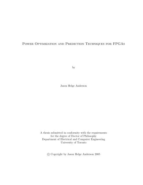
2 Background <strong>and</strong> Related WorkHDL circuitFront-end (HDL) synthesisTechnology mappingClusteringPlacementRoutingRouted circuitFigure 2.16: Typical FPGA CAD flow.tool [Chen 03]. An extension of the work appears in [Chen 04a], which proposes a new approachto register binding <strong>and</strong> port assignment that further reduces the number of multiplexer inputs,realizing additional power reductions.A recent paper by Wilton, Luk, <strong>and</strong> Ang examines the impact of pipelining on FPGA powerconsumption [Wilt 04]. The authors argue that pipelining is essentially “free” in <strong>FPGAs</strong>, due tothe large number of available registers. Since pipelining shortens combinational paths, it reducesglitches <strong>and</strong> has been successfully applied <strong>for</strong> glitch reduction in the ASIC domain [Mont 93].In [Wilt 04], the number of pipeline stages is increased gradually <strong>for</strong> each circuit in a set ofbenchmark circuits. <strong>Power</strong> reductions ranging from 40-90% are reported.Technology MappingSeveral researchers have considered power optimization during the technology mapping stepof Figure 2.16 [Farr 94, Wang 97, Li 01, Wang 01]. The key idea in power-aware technologymapping is to keep signals with high switching activity out of the power-hungry FPGA inter-34
2.5 FPGA <strong>Power</strong> <strong>Optimization</strong>LUTswitchingactivity10310 3logic functionprimary input53331 753331 7Figure 2.17: <strong>Power</strong>-aware technology mapping.connect, as illustrated in Figure 2.17. The figure shows two mapping solutions <strong>for</strong> a circuit.The nodes represent logic functions; the shaded regions represent LUTs. Switching activityvalues are shown adjacent to each signal. In the left mapping solution, the high activity signal(with activity 10) is covered within a LUT, <strong>and</strong> there<strong>for</strong>e, this signal is not required tobe routed through the interconnect. In the right mapping solution, the high activity signal isbetween LUTs <strong>and</strong> thus, must be routed through the interconnect. It is conceivable that thetwo mapping solutions have considerably different power characteristics.In an early work, Farrahi <strong>and</strong> Sarrafzadeh proposed an algorithm that minimized power atthe expense of both area <strong>and</strong> depth [Farr 94]. Their algorithm provides a 14% power improvementover an algorithm that solely optimizes area. Li, Mak, <strong>and</strong> Katkoori presented an algorithmthat optimizes power in the portions of a circuit that are not depth-critical [Li 01]. Theirapproach reduces the mapping problem to a network flow <strong>for</strong>mulation, similar to FlowMap [Cong 94a].The authors use a novel approach to translate power objectives into edge capacities in the flownetwork. In [Wang 01], the authors focused on optimizing both area <strong>and</strong> power. Their methodcomputes a set of c<strong>and</strong>idate mapping solutions <strong>for</strong> each node in an input network, <strong>and</strong> appliesa cost function to select the best solution. The approach yields mapping solutions that use 14%less power than those produced by [Farr 94], while at the same time requiring fewer LUTs.Each published technology mapping algorithm has been shown to produce mapping solutions35
2 Background <strong>and</strong> Related Workrequiring less power than solutions produced by a previously published approach. However, noneof these works has studied the trade-offs between power <strong>and</strong> other design criteria, such as areaor routability. In Chapter 5, a new power-aware technology mapping algorithm is describedthat permits trade-offs between power <strong>and</strong> depth.ClusteringAn interconnect-centric clustering algorithm was proposed in [Sing 02], <strong>and</strong> shown to offersignificant power benefits. The algorithm uses Rent’s rule [Dona 81] to create clusters withlow interconnect requirements, leading to lower overall power consumption. Previous work onclustering focused on minimizing the total number of clusters [Betz 97a]. [Sing 02] showed thatthis objective does not necessarily equate with minimizing the number of signals external toclusters – signals that ultimately impose dem<strong>and</strong> on the interconnect. The proposed algorithmuses Rent’s rule to derive a preferred upper bound on the number of pins that should beused on a cluster. An attempt is made to honor this bound during clustering, resulting in aslight increase in the average number of clusters needed to implement circuits versus [Betz 97a].However, the number of signals external to clusters is considerably reduced by this approach,leading to lower overall power.Placement <strong>and</strong> Routing<strong>Power</strong> optimization has also been considered at the placement <strong>and</strong> routing stages. [Roy 99] proposeda simulated annealing-based placer that simultaneously h<strong>and</strong>les wirelength, delay, <strong>and</strong>power minimization. <strong>Power</strong> was taken into account through an extra term in the annealingcost function. The term tallies the product of estimated capacitance <strong>and</strong> switching activity <strong>for</strong>each signal, representing the dynamic power dissipation of the current placement. In a similarway, [Roy 99] realizes power-aware routing by augmenting the router’s cost function with apower cost term. A different power-aware placement approach, based on recursive partitioning,was described in [Toga 98]. The method aims to avoid splitting high activity signals across36
2.5 FPGA <strong>Power</strong> <strong>Optimization</strong>A B Z0 0 00 1 11 0 11 1 Xz 1 = ab + abz 2 = a + bswitching activity(z 1 ) !=switching activity(z 2 )Figure 2.18: Basis of post-layout power optimization.partitions, leading to shorter wirelengths, smaller capacitances, <strong>and</strong> lower dynamic power <strong>for</strong>such signals.Post-layout <strong>Power</strong> <strong>Optimization</strong>Post-layout power optimization is possible by way of techniques that re-program LUT functionsto optimize the switching activity of signals routed through the interconnect [Kumt 00a,Hwan 98]. The aim is to exploit the concept of “don’t cares” in Boolean functions. Specifically,don’t cares give rise to alternatives in the choice of a function to be implemented by a LUT.Such alternatives may have different switching activities, <strong>and</strong> thus, offer different power characteristics.Figure 2.18 shows an example truth table with a “don’t care”, leading to two Booleanfunction alternatives, each having a different switching activity. In [Kumt 00a], a cluster ofLUTs to re-program is selected, <strong>and</strong> a neighborhood of LUTs that connect to the cluster isidentified. The cluster <strong>and</strong> its neighborhood represent a sub-circuit, H, of the entire circuit,having a specific set of inputs <strong>and</strong> outputs. Implementation alternatives <strong>for</strong> the cluster LUTsthat meet the functional requirements on the inputs <strong>and</strong> outputs of H are enumerated, <strong>and</strong>the implementation having the best power characteristics is selected. An average power reductionof 11.5% was reported [Kumt 00a]. Since the circuit is optimized “in-place”, withoutperturbing the placement or routing, the optimization is “free” from the area <strong>and</strong> per<strong>for</strong>manceperspectives.37
2 Background <strong>and</strong> Related Work<strong>Power</strong>-Aware CAD FlowThe research work noted above demonstrates that power optimization is possible at each step ofthe FPGA CAD flow. A question that arises, however, is whether the power reductions achievedat each stage are additive, or whether, <strong>for</strong> example, a power reduction achieved in technologymapping lessens the potential <strong>for</strong> power reduction at a later stage, such as placement. Thisquestion was addressed in an interesting paper by Lamoureux <strong>and</strong> Wilton, who constructed acomplete power-aware FPGA CAD flow, comprised of technology mapping, clustering, placement,<strong>and</strong> routing [Lamo 03]. Applied in isolation, the power-aware algorithms produced powerreductions of 7.6%, 12.6%, 3%, <strong>and</strong> 2.6%, respectively. When all of the algorithms were appliedsimultaneously, a total power reduction of 22.6% was observed – only slightly less than thesum of the individual power reductions (25.8%). The results suggest that the power reductionsachieved at each stage are largely orthogonal.2.6 Summary<strong>Power</strong> dissipation in CMOS circuits can be classified as either dynamic or static. Dynamic powerconsumption is due to the logic transitions that occur on a circuit’s signals during normaloperation. Static power is dissipated even when a circuit is in an idle state. Historically,dynamic power has dominated power consumption in CMOS circuits; however, technologyscaling trends have resulted in leakage becoming an increasing component of total power. Thebreakdown of power consumption in <strong>FPGAs</strong> is well-studied, <strong>and</strong> it has been observed thatinterconnect accounts <strong>for</strong> the bulk of an FPGA’s static <strong>and</strong> dynamic power. In recent years,various approaches to reducing FPGA power have been proposed in the literature, includingapproaches <strong>for</strong> leakage reduction, as well as circuit, architecture, <strong>and</strong> CAD techniques <strong>for</strong>dynamic power reduction.38
3 CAD <strong>Techniques</strong> <strong>for</strong> Leakage <strong>Optimization</strong>3.1 IntroductionThis chapter is focussed on optimizing the active leakage power dissipation of <strong>FPGAs</strong>. Recallthat active leakage refers to leakage consumed in the used <strong>and</strong> operating part of an FPGA (seeSection 2.2.2). Two novel CAD techniques <strong>for</strong> reducing active leakage are presented. Both ofthe proposed techniques are unique in that they are “no cost”, meaning that they do not worsenarea-efficiency, degrade circuit per<strong>for</strong>mance, or increase fabrication cost.The leakage consumed by a digital CMOS circuit depends on its input state. Section 3.2explores the extent to which this property holds <strong>for</strong> common FPGA hardware structures. Basedon the results observed, Section 3.3 presents a first leakage reduction approach that leveragesa specific property of the primary logic elements used in <strong>FPGAs</strong>, namely, LUTs. The propertyallows one to freely use either polarity of a logic signal, without incurring any area or delaypenalty, <strong>and</strong> without requiring modifications to the underlying FPGA hardware. Polarities arechosen <strong>for</strong> signals in a way that places hardware structures into their low leakage states.The second leakage optimization technique, described in Section 3.4, takes the leakage powerconsumptions of FPGA routing resources into account during the routing step of the CAD flow.The objective of such “leakage-aware routing” is to route design signals with a preference <strong>for</strong>using low leakage routing resources. Both of the proposed leakage reduction approaches arevalidated experimentally by applying them to optimize leakage in a 90nm Xilinx commercialFPGA. The chapter concludes with a summary in Section 3.5.39
3 CAD <strong>Techniques</strong> <strong>for</strong> Leakage <strong>Optimization</strong>i1i2s1s2SRAM celli1s1s1s1s1s1 s2s2s2s2i3s3s4i2i3s1s1s2i4i4a) decoded multiplexer b) encoded multiplexerFigure 3.1: Two 4-to-1 multiplexer implementations.3.2 FPGA Hardware StructuresMultiplexers <strong>and</strong> buffers comprise the basic building blocks of an FPGA, since they are deployedthroughout FPGA logic <strong>and</strong> interconnect. Be<strong>for</strong>e describing the proposed leakage reductionmethods, we study the leakage characteristics of such basic circuit blocks.Figure 3.1, repeated here <strong>for</strong> convenience, shows two implementation alternatives <strong>for</strong> a 4-to-1 multiplexer, one “decoded” <strong>and</strong> the other “encoded”. The trade-offs between these twodesigns were outlined in Section 2.3. To evaluate the dependence of multiplexer leakage on inputstate, SPICE simulations of both designs were per<strong>for</strong>med. The simulations were conducted at110 ◦ C using BSIM4 SPICE models <strong>for</strong> a 1.2V 90nm commercial CMOS process 1 . The selectsignals of the multiplexers were assigned values such that input i1 was selected <strong>and</strong> passed tothe multiplexer output. All 16 possible input vectors were simulated.Figure 3.2 shows the multiplexer leakage power results. A vertical bar illustrates the leakage<strong>for</strong> each input vector. Observe in Figure 3.2 that leakage power in the multiplexers is highly1 BSIM4 refers to the industry st<strong>and</strong>ard MOSFET SPICE simulation model, developed at UC Berkeley[BSIM4 04]. BSIM4 represents the state-of-the-art model. A significant enhancement of BSIM4 overBSIM3 models is the proper modeling of gate oxide leakage.40
3.2 FPGA Hardware Structuresdependent on input state. For the decoded multiplexer, the highest leakage occurs when logic-0appears on input i1 (the input whose signal is passed to the output) <strong>and</strong> logic-1 appears on allother inputs; the lowest leakage occurs when all inputs are logic-1. For the decoded multiplexer,there is a 13.7X difference in leakage power between the highest <strong>and</strong> lowest leakage states; <strong>for</strong>the encoded multiplexer, the leakage power difference is 14.2X. In addition to the leakage <strong>for</strong>each input vector, Figure 3.2 shows the average leakage power consumed when the output ofthe multiplexer is a logic-1 (solid horizontal line) <strong>and</strong> when the output of the multiplexer is alogic-0 (dashed horizontal line).Observe that, <strong>for</strong> both multiplexers in Figure 3.1, the average leakage <strong>for</strong> passing a logic-1to the multiplexer output is substantially smaller than the average leakage <strong>for</strong> passing logic-0.There are several reasons <strong>for</strong> this. First, when logic-1 (V DD ) is applied to the drain terminal ofan ON NMOS device, a “weak-1” (≈ V DD − V T H ) appears at the source terminal. The weak-1leads to reduced subthreshold leakage power in other multiplexer transistors that are OFF,versus when the potential difference across an OFF transistor is V DD [see Figure 3.3(a)]. Thisis partly due to the effect of drain-induced barrier lowering (DIBL) in short-channel transistors,which causes threshold voltage to increase (subthreshold current to decrease) when drain biasis decreased [Roy 03].In addition to affecting subthreshold leakage, another reason <strong>for</strong> the input-dependence ofthe multiplexer leakage power is the reduction in gate oxide leakage when the multiplexer ispassing logic-1 to its output. Gate leakage is a considerable fraction of total leakage in 90nmtechnology. Gate leakage in an ON NMOS transistor depends significantly on the appliedbias [Guin 03]. When an NMOS transistor is passing logic-0, the voltage difference between thegate <strong>and</strong> source is V DD (that is, V GS = V DD ) <strong>and</strong> the transistor is in the strong inversion state[see Figure 3.3(b)]. Conversely, when the transistor is passing logic-1, the transistor is in thethreshold state (V GS ≈ V T H ) [see Figure 3.3(c)]. Gate oxide leakage in the threshold state istypically several orders of magnitude smaller than in the strong inversion state [Guin 03]. Thisproperty makes it preferable to pass logic-1 (versus logic-0) from the gate leakage perspective.41
3 CAD <strong>Techniques</strong> <strong>for</strong> Leakage <strong>Optimization</strong><strong>Power</strong> (nW)60504030average powerwhen output = 0decoded multiplexeraverage powerwhen output = 1201000000:0001:0010:0011:0100:0101:0110:0111:1000:1001:1010:1011:1100:1101:1110:1111:Input vector (i1i2i3i4)6050encoded multiplexer4030201000000:0001:0010:0011:0100:0101:0110:0111:1000:1001:1010:1011:1100:1101:1110:1111:<strong>Power</strong> (nW)Input vector (i1i2i3i4)Figure 3.2: Leakage power <strong>for</strong> multiplexers.42
3.2 FPGA Hardware StructuresV DDV DDGND~= V DD- V THGNDsubthreshold leakagea) reduced subthreshold leakagegate leakageV DDGNDGNDb) high gate leakagegate leakageV DDV DDc) low gate leakage~= V DD- V THFigure 3.3: Examples of transistor leakage states.43
3 CAD <strong>Techniques</strong> <strong>for</strong> Leakage <strong>Optimization</strong>Input <strong>Power</strong> (nW)0 56.11 46.6Figure 3.4: Buffer implementation <strong>and</strong> leakage power.Another important circuit element in <strong>FPGAs</strong> is a buffer, since they are present throughoutthe routing fabric <strong>and</strong> also within logic blocks. The two stage buffer shown in Figure 3.4 wassimulated <strong>and</strong> its leakage power in both input states was evaluated. The buffer’s transistorswere sized to achieve equal rise <strong>and</strong> fall times; the second stage was chosen to be three timeslarger than the first stage. Leakage power results <strong>for</strong> the buffer are shown on the right side ofFigure 3.4. Although the difference in power between the two input states is not as pronouncedas the differences observed <strong>for</strong> the multiplexers, one can see that about 20% more power isconsumed when the buffer’s input is a logic-0 versus when its input is a logic-1. The dependenceof the buffer’s leakage on input state is a result of NMOS <strong>and</strong> PMOS devices having considerablydifferent subthreshold <strong>and</strong> gate oxide leakage characteristics, <strong>and</strong> also due to the dependenceof leakage on transistor size. For example, gate oxide leakage is considerably higher in NMOSversus PMOS transistors [Yu 00] <strong>and</strong> is also directly proportional to transistor size. There<strong>for</strong>e,overall gate leakage is minimized when the large NMOS transistor in the buffer’s second inverterstage is OFF, which occurs when the buffer’s output state is logic-1.Subthreshold leakage increases exponentially with temperature, <strong>and</strong> consequently, leakageis primarily a problem at high temperature. This work concerns active leakage power in theoperating (hot) part of the FPGA <strong>and</strong> there<strong>for</strong>e, in this chapter, the proposed leakage reductiontechniques are evaluated at high temperature (110 ◦ C). Unlike subthreshold leakage, gate oxideleakage is almost insensitive to temperature [Agar 04], making it a larger fraction of total leakage44
3.3 Active Leakage <strong>Power</strong> <strong>Optimization</strong> via Polarity Selectionat low temperature. For completeness, the leakage characteristics of the basic FPGA hardwarestructures were examined at low temperature (40 ◦ C). The results are shown in Figure 3.5.Observe that similar leakage bias trends are apparent at low temperature; namely, less leakagein consumed when logic-1 is passed through the multiplexers <strong>and</strong> buffer versus when logic-0 ispassed through these structures. In fact, in the multiplexers, the bias is more pronounced atlow temperature. For example, in the decoded multiplexer, the average leakage power whenthe output is logic-0 is 140% higher than when the output is logic-1. At high temperature, theleakage difference between the two states is only 44%. In the buffer, the same bias is presentat low temperature, but it is less pronounced; buffer leakage in the logic-0 state is about 7%higher than in the logic-1 state (versus 20% higher at high temperature).3.3 Active Leakage <strong>Power</strong> <strong>Optimization</strong> via Polarity SelectionIn Section 3.2, we observed that in a modern commercial CMOS process, the leakage powerdissipated by elementary FPGA hardware structures, namely buffers <strong>and</strong> multiplexers, is typicallysmaller when the output <strong>and</strong> input of these structures is logic-1 versus logic-0. The firstapproach to active leakage power optimization approach works by choosing a polarity <strong>for</strong> eachsignal in an FPGA design, in a manner that enables signals to spend the majority of theirtime in the logic-1 state (the logic state associated with low leakage power). A fundamentalproperty of a digital signal is its static probability, which is the fraction of time a signal spendsin the logic-1 state. A signal with static probability greater than 0.5 spends more than 50%of its time at logic-1. The leakage reduction approach alters signal polarity to achieve highstatic probability <strong>for</strong> most signals. Unlike in ASICs, signal polarity inversion in <strong>FPGAs</strong> can beachieved without any area or delay penalty, by leveraging a unique property of the basic FPGAlogic element 2 .Figure 3.6 illustrates how a signal’s polarity can be reversed in an FPGA. Part (a) of2 Changing a signal’s polarity implies a change in the direction of the signal’s logic transitions. The “no cost”property of the polarity selection optimization assumes that FPGA per<strong>for</strong>mance is not tied to the directionof logic transitions. This assumption holds <strong>for</strong> today’s commercial <strong>FPGAs</strong> from Altera <strong>and</strong> Xilinx.45
3 CAD <strong>Techniques</strong> <strong>for</strong> Leakage <strong>Optimization</strong>25decoded multiplexer20<strong>Power</strong> (nW)15105average powerwhen output = 0average powerwhen output = 100000:0001:0010:0011:0100:0101:0110:0111:1000:1001:1010:1011:1100:1101:1110:1111:Input vector (i1i2i3i4)25encoded multiplexer201510500000:0001:0010:0011:0100:0101:0110:0111:1000:1001:1010:1011:1100:1101:<strong>Power</strong> (nW)1110:1111:Input vector (i1i2i3i4)a) Leakage power <strong>for</strong> multiplexersInput <strong>Power</strong> (nW)0 19.31 18b) Leakage power <strong>for</strong> bufferFigure 3.5: Low temperature leakage power results <strong>for</strong> multiplexers <strong>and</strong> buffer (40 ◦ C).46
3.3 Active Leakage <strong>Power</strong> <strong>Optimization</strong> via Polarity Selectiona ba babint0001c dint1110c dintcd0001011000011001a) original circuit b) 2-LUT implementation c) after signal inversionFigure 3.6: LUT circuit implementation; illustration of signal inversion.the figure shows a logic circuit having two AND gates <strong>and</strong> an exclusive-OR gate. Part (b)of the figure shows the circuit mapped into 2-input LUTs. The memory contents are shown<strong>for</strong> each LUT <strong>and</strong> represent the truth table of the logic function implemented by the LUT’scorresponding gate. In this example, the aim is to invert the signal int, so that its complementedrather than its true <strong>for</strong>m is produced by a LUT <strong>and</strong> routed through the FPGA interconnectionnetwork. There are two steps to inverting a signal. First, the programming of the LUTproducing the signal must be changed. Specifically, to invert the signal, all of the 0s in itsdriving LUT must be changed to 1s <strong>and</strong> the 1s must be changed to 0s. Second, the programmingof LUTs that are fanouts of the inverted signal must be altered to “expect” the inverted <strong>for</strong>m.This is achieved by permuting the bits in the SRAM cells of such “downstream” LUTs. Part (c)of Figure 3.6 shows the circuit after the signal int is inverted. The permutation of bits in theinverted signal’s fanout LUT is shown through shading; the contents of the top two SRAMcells in the downstream LUT are interchanged with the contents of the bottom two SRAMcells in the LUT. Through this method, signal inversion in <strong>FPGAs</strong> can be achieved by simplyre-programming LUTs.47
3 CAD <strong>Techniques</strong> <strong>for</strong> Leakage <strong>Optimization</strong>function OptimizeLeakage(design, signal static probabilities)<strong>for</strong> each signal n in the design doif static_probability(n) < 0.5 thenif signal n can be inverted theninvert(n)// FPGA is re-programmed; n replaced with nreturn new designFigure 3.7: Leakage optimization algorithm.The approach to leakage power optimization is shown in Figure 3.7. The input to thealgorithm is an FPGA circuit, as well as static probability values <strong>for</strong> each signal in the circuit.A loop iterates through the signals <strong>and</strong> selects those signals having static probability less than0.5. Such signals spend most of their time in the logic-0 state, <strong>and</strong> thus, they are c<strong>and</strong>idates<strong>for</strong> inversion. For each c<strong>and</strong>idate signal, a check is made to determine if it can be inverted(discussed below). If a c<strong>and</strong>idate signal is invertible, it is inverted by re-programming the FPGAconfiguration memory accordingly. After processing all signals, the output of the algorithm is amodified design, having signals that spend the majority of their time in the logic state favourableto low leakage power.The majority of signals in FPGA designs are produced by LUTs <strong>and</strong> drive LUTs, <strong>and</strong> allsuch signals can be inverted using the approach shown in Figure 3.6. In a commercial FPGAhowever, in addition to LUTs, other types of hardware structures are usually present. Somesignals driven by or driving non-LUT structures may also be invertible, since FPGA vendorsfrequently include extra circuitry <strong>for</strong> programmable inversion. However, some signals may notbe invertible, such as those driving special control circuitry, entering the FPGA device fromoff-chip, or driving certain pins on non-LUT structures. As a concrete example, consider thatthe Xilinx Virtex-II PRO FPGA contains 18-by-18 block multipliers [Virt 03]. The inputs to48
3.3 Active Leakage <strong>Power</strong> <strong>Optimization</strong> via Polarity Selectionthe multipliers do not have programmable inversion. There<strong>for</strong>e, any signal feeding a multiplierinput should not be inverted by the proposed polarity selection approach, as doing so would befunctionally incorrect (it would change the multiplication results). Similarly, Virtex-II containslarge blocks of static RAM memory. Inverting a signal that drives a block RAM address inputis not straight<strong>for</strong>ward, as it implies a shuffling of memory contents, <strong>and</strong> block RAM memorycontents is frequently pre-loaded during an FPGA’s initial configuration phase. A two-passapproach would be needed to invert block RAM address signals: First, the polarity selectionoptimization would be executed, permitting block RAM address signal inversion. Then, thepolarity selection results would be used to determine the appropriate rearrangement of blockRAM memory contents. The memory contents would be shuffled appropriately, prior to FPGAconfiguration.Altering the polarity of a signal n with static probability P (n), changes the signal’s probabilityto 1 − P (n). There<strong>for</strong>e, <strong>for</strong> signals having static probability close to 0.5, the benefitsof inversion on leakage optimization are minimal, since the static probability of such signalsremains close to 0.5 after inversion. Low leakage power can be achieved when signals have staticprobability close to 0 or 1. A question that arises, then, is whether the signals in real circuitsexhibit this property. Below, we show that it is unlikely that the majority of signals in circuitswill have probabilities close to 0.5, which bodes well <strong>for</strong> the proposed leakage optimizationapproach.The average number of logic transitions per clock cycle on a (non-clock) signal n, F (n), canbe expressed as a function of the signal’s static probability [Ciri 87, Yeap 98]:F (n) = 2 · P (n) · [1 − P (n)] (3.1)Recall that F (n) is referred to as signal n’s normalized switching activity. Since P (n)ranges from 0 to 1, F (n) in (3.1) ranges from 0 to 0.5. Note that (3.1) is a frequently usedapproximation that becomes exact in the absence of temporal correlations in signal n’s switchingactivity. That is, (3.1) assumes that n’s values in two consecutive clock cycles are independent.49
3 CAD <strong>Techniques</strong> <strong>for</strong> Leakage <strong>Optimization</strong>Solving (3.1) <strong>for</strong> P (n), yields:P (n) = 1 ± √ 1 − 2 · F (n)2(3.2)which is plotted in Figure 3.8. Observe that P (n) is 0.5 only when F (n) is 0.5 <strong>and</strong> that <strong>for</strong> afixed decrease in F (n), there is a change in P (n) towards either 0 or 1. From Figure 3.8, onecan infer that if the switching activities of the majority of signals in circuits are not clusteredclose to 0.5, then the static probabilities of signals will also not be clustered close to 0.5.Switching activity in combinational circuits is well-studied. Prior work by Nemani <strong>and</strong> Najmfound that switching activities are generally not clustered around a single value <strong>and</strong> that onaverage, activity decreases quadratically with combinational depth in circuits [Nema 99]. Onecan there<strong>for</strong>e expect there to be a range of different static probabilities amongst the signals ofa circuit <strong>and</strong> that “deeper” signals in circuits will have static probabilities approaching either0 or 1. This analysis suggests that <strong>for</strong> many signals, changing polarity will have a significantimpact on leakage power.Often, design verification is done at the post-routing stage, through HDL simulation withextracted routing delays, or by using logic analyzers, such as Xilinx ChipScope [XilinxCh 04].ChipScope is an IP core that is inserted within a user’s FPGA design. It allows one to view thestates of the design’s internal signals during execution on the FPGA hardware. The presenceof the polarity selection optimization within the CAD flow may complicate such verification.Specifically, the inversion of some signals may make verification results unintelligible to users.This is analogous to the effect that compiler optimizations have on one’s ability to run adebugger on optimized code in software development. In this case, however, a simple workaroundis available: the verification tools can be made “aware” of which signals have beeninverted, <strong>and</strong> can present the “true” <strong>for</strong>m of signals to users, as appropriate.50
3.3 Active Leakage <strong>Power</strong> <strong>Optimization</strong> via Polarity Selection10.8- P(n)Static probability0.60.40.200 0.05 0.1 0.15 0.2 0.25 0.3 0.35 0.4 0.45 0.5Switching activity - F(n)Figure 3.8: Static probability versus switching activity.3.3.1 Experimental Study <strong>and</strong> ResultsThe effectiveness of the proposed leakage power reduction approach was gauged by applying it tooptimize active leakage in the Xilinx Spartan-3 1.2V 90nm commercial FPGA. The breakdownof leakage in Spartan-3 has recently been studied by other authors [Tuan 03].describes the experimental methodology <strong>and</strong> subsequently, provides results.This sectionMethodologyThe target FPGA is composed of an array of configurable logic block (CLB) tiles, I/Os, <strong>and</strong>other special-purpose blocks, such as multipliers <strong>and</strong> block RAMs. Smaller versions of theFPGA contain only the CLB array <strong>and</strong> I/Os. An embedded version of the FPGA, containingthe CLB array only, is also available <strong>for</strong> incorporation into custom ASICs. In this chapter, thefocus is on leakage optimization within the FPGA’s CLB array, which represents the bulk ofthe FPGA’s silicon area, especially in smaller devices <strong>and</strong> the embedded version. The non-CLBblocks (e.g., block RAMs) are not unique to <strong>FPGAs</strong>; leakage optimization in these blocks has51
3 CAD <strong>Techniques</strong> <strong>for</strong> Leakage <strong>Optimization</strong>Table 3.1: Major circuit blocks in target FPGA.Circuit blockIMUXDIRECTDOUBLEHEXLONGLUTFLIP-FLOPDetails30-to-1 multiplexer, buffer24-to-1 multiplexer, buffer16-to-1 multiplexer, buffer12-to-1 multiplexer, buffern-to-1 multiplexer, buffer(n device/orientation dependent)16-to-1 multiplexer, in/out buffersprogrammable set/resetbeen studied in other contexts.A Spartan-3 CLB tile contains both logic <strong>and</strong> routing resources <strong>and</strong> is similar to a Virtex-4CLB, shown in Figure 2.9. The CLB’s logic resources consist of four logic sub-blocks, calledSLICEs. Each SLICE contains two 4-LUTs, two flip-flops, as well as arithmetic <strong>and</strong> othercircuitry. Like Virtex-4, the Spartan-3 interconnect consists of variable length wire segmentsthat connect to one another through programmable, buffered switches similar to that shownin Figure 2.10. Table 3.1 provides further detail on the major circuit blocks in the Spartan-3CLB tile, including the widths of the interconnect multiplexers. The input multiplexer (IMUX)selects <strong>and</strong> routes a signal to a SLICE input pin. The DIRECT interconnect block selects <strong>and</strong>routes a signal from a SLICE output pin to a neighboring logic block. DOUBLE blocks drivewire segments that span 2 CLB tiles. HEX blocks drive wires that span 6 CLB tiles. LONGresources span the entire width or height of the FPGA. Note that a single CLB tile containsmultiple instances of each of the blocks listed in Table 3.1.Figure 3.9 shows the leakage optimization <strong>and</strong> analysis flow. As mentioned in Section 3.3,the input to the optimization algorithm is an FPGA circuit, as well as the static probabilityvalue <strong>for</strong> each of the circuit’s signals. The benchmark circuits consist of 10 large combinationalMCNC circuits <strong>and</strong> 6 industrial circuits collected from Xilinx customers; the circuits are listed52
3.3 Active Leakage <strong>Power</strong> <strong>Optimization</strong> via Polarity Selectionin Table 3.2 3 . The MCNC circuits were first synthesized from VHDL using Synplicity’s SynplifyPro tool (version 7.0). Then, the circuits were technology mapped, placed, <strong>and</strong> routed in thetarget FPGA using the Xilinx software tools (version M6.2i).The industrial circuits werealready available in technology mapped <strong>for</strong>m so only the placement <strong>and</strong> routing steps wererequired <strong>for</strong> these circuits.An earlier version of this work presented preliminary results <strong>for</strong> circuits that were notoptimized <strong>for</strong> speed per<strong>for</strong>mance [Ande 04f]. In practice, however, most FPGA users seek ahigh per<strong>for</strong>mance design implementation. Consequently, the Xilinx place <strong>and</strong> route tools wereused to generate a per<strong>for</strong>mance-optimized layout <strong>for</strong> each design as follows: First, each designwas placed <strong>and</strong> routed with an easy-to-meet timing (critical path delay) constraint; then, basedon the per<strong>for</strong>mance achieved, a more aggressive constraint was generated, <strong>and</strong> the place <strong>and</strong>route tools were re-executed using the new constraint. The entire process was repeated until aconstraint that could not be met by the layout tools was encountered. The proposed leakagereduction technique is evaluated <strong>for</strong> the layout solution corresponding to the most aggressive,but achievable, constraint observed throughout the entire iterative process.To gather static probability data, the routed circuits were simulated using either the SynopsysVHDL System Simulator (VSS) (version 2000.06) or Mentor Graphics’ ModelSIM (version5.7a). The simulators have built-in capabilities <strong>for</strong> capturing the fraction of time a signalspends at logic-1 (static probability). Representative simulation vectors <strong>for</strong> the circuits werenot available, <strong>and</strong> there<strong>for</strong>e, the circuits were simulated using 10,000 r<strong>and</strong>omly chosen inputvectors. Clock <strong>and</strong> control inputs in the industrial circuits were identified by examining loadpin types <strong>and</strong> by inferring functionality based on signal names. Such clock/control inputs werepresented with appropriate, non-r<strong>and</strong>om signals in the simulations. For the control inputs, atrial-<strong>and</strong>-error approach was used to select between applying an “active high” or an “activelow” input wave<strong>for</strong>m. Note that the 6 industrial circuits were selected from an initial, largerpool of circuits, from which the balance had to be eliminated due to a lack of knowledge re-3 The industrial circuits are single clock designs. Multi-clock designs were not used, since, <strong>for</strong> such designs, therelationship between clock signals is difficult to determine without access to user-provided simulation vectors.53
3 CAD <strong>Techniques</strong> <strong>for</strong> Leakage <strong>Optimization</strong>Table 3.2: Characteristics of benchmark circuits.Circuit LUTs FFsalu4 500 0apex4 1078 0cps 524 0dalu 323 0ex1010 1112 0ex5p 557 0misex3 257 0pdc 609 0seq 1193 0spla 229 0industry1 1511 2128industry2 1654 1278industry3 2818 368industry4 2942 1262industry5 8676 5507industry6 4895 318garding their internal functionality. For such eliminated circuits, it was not possible to identifya simulation vector set that realized toggling on a significant fraction of each circuit’s internalsignals.In the r<strong>and</strong>omly generated input vectors, the probability of each primary input toggling betweensuccessive vectors was set to 50%. Note that, given the static probabilities of a circuit’sprimary input signals, the static probabilities of the circuit’s internal signals can be computedusing well-known probabilistic techniques [Yeap 98]. Thus, simulation is not a requirement <strong>for</strong>the use of the optimization approach, <strong>and</strong> it is expected that the approach could be incorporatedinto EDA tools that automatically per<strong>for</strong>m the proposed leakage optimization. Certainly,it seems possible that the static probabilities initially known <strong>and</strong> supplied to the proposedalgorithm may differ from those probabilities actually experienced by the circuit in the field.This potential issue can be addressed easily since the polarity selection optimization does notdisrupt placement, routing, or design per<strong>for</strong>mance. One can freely re-apply the algorithm whenan updated set of static probabilities is available, <strong>and</strong> the resulting updated bitstream can thenbe used to re-program an already-deployed FPGA design in the field.54
3.3 Active Leakage <strong>Power</strong> <strong>Optimization</strong> via Polarity SelectionMCNC HDL circuitHDL synthesis (Synplify Pro)FPGA vendor toolsTechnology mappingPlacement <strong>and</strong> routingRouted designIndustrial circuitDevice usage analysisDesign usage dataSimulation (VSS or ModelSIM)Static probability dataLeakage <strong>Optimization</strong> (Optional)Static probability dataSimulationvectors<strong>Power</strong> analysis scriptActive leakage power <strong>for</strong> designCircuit blockleakage data(from SPICE)Figure 3.9: Leakage analysis flow.55
3 CAD <strong>Techniques</strong> <strong>for</strong> Leakage <strong>Optimization</strong>SPICE simulations were per<strong>for</strong>med <strong>for</strong> each type of circuit block in the FPGA’s CLB tile.The leakage power consumed by each block <strong>for</strong> each of its possible input vectors was captured.Circuit regularity permitted the blocks with many inputs to be partitioned into sub-blocks,which were then simulated independently. To illustrate, consider a 16-to-1 multiplexer, constructedusing four 4-to-1 multiplexer in a “first stage”, <strong>and</strong> a fifth 4-to-1 multiplexer in a“second stage”. One need not simulate all 2 16 input combinations of the 16-to-1 multiplexerto gather accurate leakage data <strong>for</strong> each of these input combinations. One can simulate theindividual 4-to-1 multiplexers <strong>and</strong> combine their leakage results to produce leakage data <strong>for</strong>the large 16-to-1 multiplexer. This was the approach taken to gather leakage data <strong>for</strong> thecommercial blocks with many inputs. Notably, we observed the leakage characteristics of thecommercial FPGA’s circuit blocks to be similar to those of the generic structures studied inSection 3.2.The total active leakage power, L active , was computed twice <strong>for</strong> each benchmark circuit,both with <strong>and</strong> without the proposed optimization technique. L active is defined as the sum ofthe leakage power in each used circuit block. By analyzing the routed FPGA implementation<strong>for</strong> a benchmark, one can determine its circuit block usage, including the signals on the inputs<strong>and</strong> outputs of each used circuit block.Computing the leakage <strong>for</strong> a used instance of a circuit block in a benchmark involves combiningthe power data extracted from the block’s SPICE simulation with usage data from thebenchmark circuit’s FPGA implementation <strong>and</strong> static probability data from the benchmark’sHDL simulation. It is worth rein<strong>for</strong>cing that we do not use the power data presented in Section3.2 in the experimental study; rather, the results here are based on power data extractedfrom SPICE simulations of the commercial FPGA’s circuit blocks.Consider a used instance B of a circuit block in a benchmark <strong>and</strong> let ⃗v B represent an inputvector that may be presented to block B. Each bit i in vector ⃗v B , ⃗v B (i), corresponds to aninput i on block B. Let S B (i) represent the signal on input i of block B in the benchmark’sFPGA implementation. The static probability of signal S B (i), P (S B (i)), is a known quantity,56
3.3 Active Leakage <strong>Power</strong> <strong>Optimization</strong> via Polarity Selectionextracted from the benchmark’s HDL simulation. If bit ⃗v B (i) is logic-1 in vector ⃗v B , then wedefine the static probability of bit ⃗v B (i), P (⃗v B (i)), to be equal to P (S B (i)). On the otherh<strong>and</strong>, if ⃗v B (i) is logic-0 in ⃗v B , then P (⃗v B (i)) is defined to be 1 − P (S B (i)). One can computethe probability of vector ⃗v B appearing on the inputs of block B, P (⃗v B ), as the product of itsconstituent bit probabilities:∏P (⃗v B ) = P (⃗v B (i)) (3.3)⃗v B (i) ɛ ⃗v BNote that it is entirely possible that some inputs to a used circuit block may have nosignal on them. For example, some inputs to a routing switch (see Figure 2.10) may attachto conductors that are not used in the FPGA implementation of a benchmark circuit. In acommercial FPGA, unused routing conductors are not allowed to “float” to an indeterminatevoltage state. In the target Xilinx FPGA, unused routing conductors are pulled up to logic-1.Pulling unused routing conductors into the low leakage, logic-1 state benefits overall leakagein the FPGA, since an FPGA implementation of a benchmark circuit requires only a fractionof the FPGA’s routing resources. To demonstrate this, a detailed analysis of a portion ofthe routing in the industry4 benchmark was per<strong>for</strong>med. In industry4’s routing, we found thatthere were 15,235 used DOUBLE resources, <strong>and</strong> 5,918 used HEX resources. On average, 10.4(of 16) inputs on each DOUBLE resource in industry4’s routing attached to unused routingconductors. The remaining 5.6 inputs (on average) attached to routing conductors with anactive logic signal on them; that is, 5.6 inputs attached to routing conductors that were usedin the routing of industry4. Likewise, the HEX resources in industry4 had 7.6 (of 12) inputsattached to unused routing conductors, on average, with the remaining 4.4 inputs attached toused routing conductors. In other words, considering all HEX <strong>and</strong> DOUBLE resources used inindustry4, nearly 2/3 of the inputs to these resources attach to unused routing conductors, <strong>and</strong>are there<strong>for</strong>e pulled to logic-1. This amplifies the need <strong>for</strong> the “prefer logic-1” approach takenin the polarity selection optimization.57
3 CAD <strong>Techniques</strong> <strong>for</strong> Leakage <strong>Optimization</strong>signal X I1signal Y I2BP(X) = 0.25, P(Y) = 0.33I1 I2 POWER0 0 50 1 61 0 81 1 10from SPICEsimulationsfrom benchmark’s HDL simulationL active(B) = (1 - 0.25)•(1 - 0.33)•5 + (1 - 0.25) •0.33•6 +0.25•(1 - 0.33) •8 + 0.25•0.33*10 = 6.1Figure 3.10: Example active leakage power computation.The average active leakage power <strong>for</strong> a used circuit block B, L active (B), is computed as aweighted sum of the leakage power consumed by B <strong>for</strong> each of its input vectors:L active (B) =∑P (⃗v B ) · L active (⃗v B ) (3.4)⃗v B ɛ V Bwhere V B represents the set of all possible input vectors <strong>for</strong> circuit block B, <strong>and</strong> L active (⃗v B )represents the leakage power consumed by block B when its input state is vector ⃗v B , obtainedfrom SPICE simulations.An example of the leakage power computation approach <strong>for</strong> a block with two inputs is shownin Figure 3.10. In the example, the signal, X, on block input I1 has a static probability of 0.25<strong>and</strong> the signal, Y , on input I2 has a static probability of 0.33. A table gives the power consumedby the block <strong>for</strong> each possible input vector. Consider, <strong>for</strong> example, the vector in which I1 = 1<strong>and</strong> I2 = 0. The leakage power consumed by the block <strong>for</strong> this vector is 8. The probability ofthe vector appearing on the inputs of the block is: P (X)·[1−P (Y )] = 0.25·(1−0.33) = 0.1675.Thus, the contribution of this vector to the block’s active leakage is 0.1675 · 8 = 1.34, which isthe third term in the equation shown in Figure 3.10.Leakage power was not a primary design consideration in the target commercial FPGA.58
3.3 Active Leakage <strong>Power</strong> <strong>Optimization</strong> via Polarity SelectionWe envision that the proposed active leakage reduction approach will be used in conjunctionwith a future, leakage-optimized FPGA architecture. Consequently, the experimental resultspresented here consider only the active leakage power <strong>and</strong> ignore leakage in the unused partsof the FPGA. Reducing unused leakage can be viewed as a separate optimization problem thatcan be addressed by either powering down the unused circuit blocks, by applying the st<strong>and</strong>byleakage optimization techniques mentioned in Section 2.2.2, or through circuit techniques thatwill be introduced in the next chapter. Moreover, the results do not include the leakage inthe FPGA’s SRAM configuration cells. As observed in Section 2.4.2 (page 27), the contentsof such cells changes only during the initial FPGA configuration phase, <strong>and</strong> thus, their speedper<strong>for</strong>mance is not critical. In a future low leakage FPGA, the SRAM configuration cells canbe slowed down, <strong>and</strong> their leakage greatly reduced.ResultsWe begin by comparing the active leakage power consumed in the unoptimized circuits withthat consumed in the optimized circuits. Figure 3.11 shows the percentage reduction in activeleakage power <strong>for</strong> each circuit. The improvement ranges from 15% to 38%, with the averagebeing 25%. The power benefits observed are quite substantial, considering that the proposedoptimization has no impact on circuit area or delay <strong>and</strong> requires no hardware changes.Table 3.3 gives the detailed power results <strong>for</strong> each circuit. Columns 2-4 give power data <strong>for</strong>the unoptimized circuits. Columns 2 <strong>and</strong> 3 present the power dissipated in the interconnect<strong>and</strong> non-interconnect (labeled “other”) circuit blocks, respectively. Column 4 presents the totalactive leakage power <strong>for</strong> each circuit. Columns 5-7 present analogous data <strong>for</strong> the optimizedcircuits. In these columns, percentage improvement values, relative to the unoptimized circuits,are shown in parentheses. From Table 3.3, one can see that the proposed optimization is moreeffective at reducing leakage in the interconnect versus the non-interconnect circuit blocks. Thenon-interconnect blocks include LUTs, flip-flops, <strong>and</strong> other circuitry. A more in-depth analysisrevealed that flip-flop leakage power was only slightly dependent on whether the flip-flop was59
3 CAD <strong>Techniques</strong> <strong>for</strong> Leakage <strong>Optimization</strong>45Leakage power reduction (%)403530252015105avg = 25.3%0alu4apex4cpsdaluex1010ex5pmisex3pdcseqsplaindustry1industry2industry3industry4industry5industry6Figure 3.11: Leakage power reduction results.Table 3.3: Detailed active leakage power results.UnoptimizedOptimizedInterconnect Other Total Interconnect Other TotalCircuit (µW) (µW) (µW) (µW) (%) (µW) (%) (µW) (%)alu4 690 193 883 494 (28.4) 187 (3.1) 681 (22.8)apex4 1625 415 2040 1060 (34.8) 410 (1.2) 1470 (27.9)cps 698 183 881 476 (31.8) 180 (1.6) 656 (25.6)dalu 465 126 591 341 (26.7) 125 (0.8) 466 (21.1)ex1010 1747 427 2174 1045 (40.2) 424 (0.7) 1469 (32.4)ex5p 829 210 1039 432 (47.8) 210 (0.0) 642 (38.2)misex3 295 99 394 222 (24.8) 97 (2.0) 319 (19.1)pdc 854 235 1089 598 (30.0) 230 (2.1) 828 (24.0)seq 1895 453 2348 1335 (29.6) 451 (0.4) 1786 (23.9)spla 315 89 404 239 (24.1) 87 (2.2) 326 (19.3)industry1 3415 1557 4972 2164 (36.7) 1530 (1.7) 3693 (25.7)industry2 2392 1340 3732 1408 (41.1) 1306 (2.6) 2713 (27.3)industry3 4987 1573 6560 4086 (18.1) 1558 (0.9) 5644 (14.0)industry4 6856 1927 8782 3531 (48.5) 1856 (3.7) 5386 (38.7)industry5 14696 6486 21183 10657 (27.5) 6412 (1.1) 17069 (19.4)industry6 6429 3524 9953 3919 (39.0) 3464 (1.7) 7382 (25.8)Average: 33.1% 1.6% 25.3%60
3.3 Active Leakage <strong>Power</strong> <strong>Optimization</strong> via Polarity Selectionstoring a 0 or a 1. Consequently, flip-flop leakage is not affected substantially by the proposedmethod. Similarly, it was observed that the LUTs in the target FPGA contain additional inputbuffers <strong>and</strong> other circuitry that make their leakage less sensitive to their input state. In theunoptimized circuits, 24% of active leakage power is dissipated in the non-interconnect circuitblocks <strong>and</strong> 76% in the interconnect blocks, on average. In the optimized circuits, 32% of leakageis attributable to non-interconnect blocks.The results in Table 3.3 show a wide variation in improvement across the circuits. This canbe partially explained by considering the distribution of static probabilities amongst a circuit’ssignals. The proposed technique offers the greatest benefit in circuits having many signalswith low static probability, <strong>and</strong> the least benefit in circuits having many signals with staticprobability ≥ 0.5, as these signals are already in the low leakage state. Note that the staticprobability of a signal in a circuit is a function of both the simulation vector set, as well as thecircuit’s logic functionality. According to the data in Table 3.3, the best results were achieved<strong>for</strong> the circuit industry4, with leakage reduced by 38%. Figure 3.12(a) shows a histogram ofstatic probabilities in this circuit, extracted from the ModelSIM simulation. The horizontalaxis represents static probability; the vertical axis represents the fraction the circuit’s signalshaving static probability in a specific range. Observe that, <strong>for</strong> this circuit, the majority ofsignals have low static probability, with more than 60% of signals having probability less than0.1. We verified that the skewed distribution was not a result of the simulation vector set failingto adequately exercise the circuit. In fact, more than 90% of the signals in circuit industry4experienced toggling during its simulation. Figure 3.12(b) shows the histogram <strong>for</strong> the circuitindustry3, <strong>for</strong> which the worst leakage reduction results were observed. Here, it is apparentthat many signals have static probability close to 0.5. For such signals, the static probabilityremains close to 0.5 after inversion, limiting the benefit of the leakage reduction approach.Further characterization <strong>and</strong> control of static probability in FPGA circuits is a direction <strong>for</strong>future work.61
3 CAD <strong>Techniques</strong> <strong>for</strong> Leakage <strong>Optimization</strong>706050% of signals403020100[0.0:0.1][0.1:0.2][0.2:0.3][0.3:0.4][0.4:0.5][0.5:0.6][0.6:0.7][0.7:0.8][0.8:0.9][0.9:1.0]Static probabilitya) circuit industry4706050% of signals403020100[0.0:0.1][0.1:0.2][0.2:0.3][0.3:0.4][0.4:0.5][0.5:0.6][0.6:0.7][0.7:0.8][0.8:0.9][0.9:1.0]Static probabilityb) circuit industry3Figure 3.12: Histograms of static probability.62
3.4 Active Leakage <strong>Power</strong> <strong>Optimization</strong> via Leakage-Aware Routing3.4 Active Leakage <strong>Power</strong> <strong>Optimization</strong> via Leakage-AwareRoutingThis section introduces a second approach to active leakage optimization, referred to as “leakageawareFPGA routing”. The idea is based on two observations:1. Different routing switch types in an FPGA have different leakage power consumptions.For example, as illustrated in Table 3.1, some switch types have wider input multiplexersor larger buffers than other switch types, leading to higher average leakage.2. Between any two logic block pins in an FPGA, there exist a variety of different routingpaths, comprised of different routing switch types. The routing step of the CAD flowis tasked with selecting a path between the driver <strong>and</strong> load pin(s) <strong>for</strong> each of a design’ssignals.FPGA routers employ a cost function <strong>and</strong> aim to find low-cost paths through the routingfabric from each signal’s source pin to its load pin(s) [McMu 95, Swar 98]. The cost of a completerouting path is defined to be the sum of the costs of the path’s constituent routing resources(switches). A cost function associates a particular cost value with each routing resource in theFPGA. Cost values can be chosen based on any number of criteria, <strong>for</strong> example, delay, scarcity,capacitance, or congestion. The main idea in leakage-aware routing is to select the cost <strong>for</strong>each routing resource in proportion to the resource’s leakage power consumption, <strong>and</strong> then touse such costs during routing. The intent is to associate higher costs with more “leaky” switchtypes, making them less likely to be selected during routing, ultimately producing routingsolutions having lower active leakage power consumptions.The router in the Xilinx CAD flow classifies a design’s driver/load connections as eithercritical or non-critical, based on their timing slack relative to the design’s per<strong>for</strong>mance constraints.Critical <strong>and</strong> non-critical connections are then routed in timing-driven or cost-drivenmode, respectively [Ande 04a]. In timing-driven mode, detailed RC delay calculations are used63
3 CAD <strong>Techniques</strong> <strong>for</strong> Leakage <strong>Optimization</strong>during routing to minimize driver/load connection delay. In cost-driven mode, each routingresource is given a specific cost, as mentioned above, <strong>and</strong> the router attempts to minimize thetotal path cost <strong>for</strong> a given driver/load connection. The specific resource cost assignment usedwithin the Xilinx router is proprietary; however, it reflects a combination of delay, wirelength,<strong>and</strong> scarcity. The original, unmodified Xilinx router is referred to as the baseline router.The proposed leakage-aware routing approach can be applied in t<strong>and</strong>em with the polarityselection optimization described in Section 3.3. Consequently, the optimized circuits (optimizedthrough polarity selection) were used to derive a set of new, leakage-aware routing resourcecosts. The leakage of each used routing resource in the optimized circuits was analyzed, <strong>and</strong>from this, the average leakage of each routing resource type was computed. The results areshown in Figure 3.13, normalized to the leakage consumed by a DOUBLE resource. Observethat the average leakage of a HEX resource, which spans 6 CLB tiles, is slightly lower than thatof a DOUBLE resource, which spans 2 CLB tiles, implying that on a leakage basis, using a HEXshould be “cheaper” than using a DOUBLE 4 . This relative costing is counter to other traditionalcosting criteria, such as wirelength, in which the cost of a HEX would be set considerably higherthan the cost of a DOUBLE.The Xilinx router was modified by altering the cost values used in cost-driven mode. Specifically,the cost of each routing resource was set to be proportional to the average leakage ofits routing resource type. Since the aim here is to reduce leakage without compromising per<strong>for</strong>mance,we continue to allow the router to route timing-critical connections in timing-drivenmode. Only non-critical connections are routed using the new leakage-derived costs. Themodified router is referred to as the leakage-aware router.4 A routing resource that drives a long wire segment may consume less leakage than some other resource thatdrives a short wire segment. This is possible since switch leakage does not depend on the metal segmentlength. Rather, leakage depends on the switch multiplexer size <strong>and</strong> structure, <strong>and</strong> transistor sizings in themultiplexer <strong>and</strong> buffer.64
3.4 Active Leakage <strong>Power</strong> <strong>Optimization</strong> via Leakage-Aware RoutingNormalized average leakage power2.521.510.50DOUBLE IMUX OMUX HEX LONGRouting resource typeFigure 3.13: Average leakage of routing resource types.3.4.1 Experimental Study <strong>and</strong> ResultsUsing the leakage-aware router, we again target the 90nm commercial FPGA described in Section3.3.1 with the same set of 16 benchmark circuit designs. To begin with, the proceduredescribed in Section 3.3.1 was repeated that computes an aggressive, but feasible, timing constraint<strong>for</strong> each design. The constraints achieved using the leakage-aware router were comparedwith those achieved using the baseline router. The results are shown in Table 3.4. Columns 2<strong>and</strong> 3 show the critical path delay constraint <strong>for</strong> each circuit, routed using the baseline <strong>and</strong>leakage-aware routers, respectively. Note that the same placer was used in both cases. Theparentheses in column 3 show the percentage degradation in per<strong>for</strong>mance when the leakageawarerouter is used versus the baseline router. Ten of the 16 circuits experienced a slightper<strong>for</strong>mance degradation, though no degradation was larger than 4%. The per<strong>for</strong>mance of theremaining 6 circuits actually improved slightly (negative values in the table). Changes to therouter’s cost function lead to variability in the routing solutions produced, resulting in per<strong>for</strong>-65
3 CAD <strong>Techniques</strong> <strong>for</strong> Leakage <strong>Optimization</strong>Table 3.4: Effect of leakage-aware routing on critical path delay.Baseline routing Leakage-aware routingper<strong>for</strong>mance (ns) per<strong>for</strong>mance (ns)Circuit(% degradation)alu4 11.05 11.12 (0.6)apex4 14.31 14.79 (3.4)cps 11.59 11.90 (2.7)dalu 11.43 11.32 (-0.9)ex1010 21.84 22.08 (1.1)ex5p 12.92 12.32 (-4.6)misex3 11.89 11.53 (-2.9)pdc 13.93 13.63 (-2.0)seq 13.30 13.55 (1.9)spla 10.76 10.91 (1.4)industry1 4.63 4.51 (-2.6)industry2 10.83 10.78 (-0.5)industry3 16.79 17.19 (2.3)industry4 4.83 4.94 (2.1)industry5 5.13 5.23 (2.0)industry6 21.86 22.07 (1.0)AverageDegradation: 0.3%mance improvements in some cases. On average, the degradation across all circuits was 0.3%,which we consider to be noise. One can there<strong>for</strong>e conclude that any reductions in leakage poweroffered by leakage-aware routing do not come at the expense of speed per<strong>for</strong>mance. As with thepolarity selection optimization presented in Section 3.3, leakage-aware routing is a “no cost”leakage reduction technique.The polarity selection optimization was applied in conjunction with leakage-aware routing,<strong>and</strong> the leakage in the resultant circuits was computed. Leakage was computed using the sameapproach described in Section 3.3.1. Figure 3.14 summarizes the results observed <strong>and</strong> illustratesthe reduction in leakage in the optimized versus unoptimized circuits. Each bar in the figurerepresents the percentage reduction in leakage <strong>for</strong> a given circuit; the bars are partitioned toshow the portion of the total reduction due to the polarity selection <strong>and</strong> leakage-aware routingoptimizations, respectively. The average reduction across all circuits is 30.2%. Though the bulk66
3.4 Active Leakage <strong>Power</strong> <strong>Optimization</strong> via Leakage-Aware Routing50Leakage power reduction (%)45403530252015105avg = 30.2%Leakage-aware routingPolarity selection0alu4apex4cpsdaluex1010ex5pmisex3pdcseqsplaindustry1industry2industry3industry4industry5industry6Figure 3.14: Leakage power reduction results <strong>for</strong> combined polarity selection <strong>and</strong> leakage-awarerouting.of the power reduction is due to the polarity selection optimization, the benefits of leakage-awarerouting are nonetheless substantial, especially in the industrial benchmark circuits.Detailed leakage power results <strong>for</strong> each circuit are shown in Table 3.5. Columns 2 <strong>and</strong> 3give data <strong>for</strong> the interconnect <strong>and</strong> non-interconnect (labeled “other”) circuit blocks, respectively.Column 4 gives the total active leakage power. The numbers in parentheses are percentage improvementvalues that show the reduction in leakage power relative to the unoptimized circuits;they compare the data in Table 3.5 with the data in columns 2 through 4 of Table 3.3. Noticethat, as expected, only leakage in the interconnect circuit blocks is affected by leakage-awarerouting; leakage in the “other” circuit blocks is unchanged versus using the polarity selectionoptimization alone (see column 6 of Table 3.3). For the MCNC circuits, the average reductionin total active leakage was 29.4%.In the industrial circuits, larger leakage reductionswere observed, with the average reduction being 31.6%, due primarily to larger reductions ininterconnect leakage <strong>for</strong> these circuits. The circuit industry4 experienced the largest leakagereduction of nearly 44%. Column 5 of Table 3.5 shows the percentage improvement in leakage67
3 CAD <strong>Techniques</strong> <strong>for</strong> Leakage <strong>Optimization</strong>Table 3.5: Detailed active leakage power results <strong>for</strong> leakage-aware routing combined with polarityselection.% improvementInterconnect Other Total versus polarityCircuit (µW) (%) (µW) (%) (µW) (%) selection alonealu4 460 (33.3) 187 (3.1) 647 (26.7) 5.0apex4 953 (41.4) 410 (1.2) 1363 (33.2) 7.3cps 434 (37.9) 180 (1.6) 614 (30.3) 6.4dalu 341 (26.7) 125 (0.8) 466 (21.2) 0.7ex1010 972 (44.4) 424 (0.7) 1396 (35.8) 5.0ex5p 431 (48.0) 210 (0.0) 641 (38.3) 0.2misex3 201 (31.6) 97 (2.0) 298 (24.2) 6.3pdc 542 (36.5) 230 (2.1) 772 (29.1) 6.7seq 1177 (37.9) 451 (0.4) 1628 (30.7) 8.8spla 217 (31.3) 87 (2.2) 304 (24.9) 7.0industry1 1840 (46.1) 1530 (1.7) 3369 (32.2) 8.8industry2 1191 (50.2) 1306 (2.6) 2497 (33.1) 8.0industry3 3515 (29.5) 1558 (0.9) 5073 (22.7) 10.1industry4 3085 (55.0) 1856 (3.6) 4941 (43.7) 8.3industry5 9404 (36.0) 6412 (1.1) 15816 (25.3) 7.3industry6 3268 (49.2) 3464 (1.7) 6731 (32.4) 8.8Average (MCNC): 36.9% 1.4% 29.4% 5.3%Average (Industrial): 44.3% 2.0% 31.6% 8.5%relative to applying the polarity selection optimization alone. That is, the data in column 5compares the leakage numbers in column 4 with the leakage numbers in column 7 of Table 3.3.On average, leakage-aware routing provides a 5.3% leakage reduction in the MCNC circuits,<strong>and</strong> an 8.5% reduction in the industrial circuits. In summary, the results show that the additionalleakage power reductions offered by leakage-aware routing are considerable, especiallygiven that the approach involves software changes only, <strong>and</strong> imposes no hardware, fabrication,or per<strong>for</strong>mance cost.As mentioned above, the cost of a HEX resource in the leakage-aware router is similar tothat of a DOUBLE resource. Whereas, in the baseline router, the cost of HEX is higher thanthat of a DOUBLE. Certainly, leakage-aware routing leads to higher HEX utilization, <strong>and</strong>, sincethe capacitance of a HEX is larger than that of a DOUBLE, it is conceivable that leakage-aware68
3.5 Summaryrouting may increase dynamic power consumption. A future research direction is to investigatethis possibility, <strong>and</strong>, if deemed a problem, to enhance leakage-aware routing to account <strong>for</strong> it,perhaps by taking signal switching activity into account when deciding how a signal shouldbe routed. That being said, we anticipate that the proposed techniques will be applied in afuture low leakage FPGA, perhaps implemented in 65 or 45nm process technology. At suchtechnology nodes, we expect that leakage power, not dynamic power, will be the overridingpower consideration.3.5 SummaryThis chapter presented two “no cost” approaches to active leakage power reduction in <strong>FPGAs</strong>.The leakage power characteristics of common FPGA hardware structures were studied, <strong>and</strong>it was observed that their leakage depends strongly on the state of their inputs. A novelapproach to leakage power reduction was proposed, in which polarities are selected <strong>for</strong> logicsignals to place hardware structures into low leakage states, as much as possible. The techniqueis based on a unique property of FPGA logic elements (LUTs) that permits either the true orcomplemented <strong>for</strong>m of a signal to be generated, without any area or delay penalty. Experimentalresults <strong>for</strong> a 90nm state-of-the-art commercial FPGA show that the proposed approach reducesactive leakage by 25%, on average. Subsequently, the concept of leakage-aware routing wasintroduced, in which the cost function used during the routing step of the CAD flow is alteredto consider the leakage power consumptions of routing resources. Leakage-aware routing incursno significant per<strong>for</strong>mance penalty, <strong>and</strong> offers additional leakage reductions. Combining the twotechniques produces a total active leakage reduction of up to 44%, with the average reductionbeing 30%.69
3 CAD <strong>Techniques</strong> <strong>for</strong> Leakage <strong>Optimization</strong>70
4 Circuit <strong>Techniques</strong> <strong>for</strong> Low-<strong>Power</strong> Interconnect4.1 IntroductionInterconnect plays a dominant role in the dynamic <strong>and</strong> static (leakage) power dissipation of<strong>FPGAs</strong>. In comparison with custom ASICs, FPGA interconnect presents a high capacitiveload, due to the presence of lengthy pre-fabricated wire segments <strong>and</strong> the programmable routingswitches attached to each wire. Dynamic power scales in direct proportion to amount ofcapacitance switched in a logic transition. Leakage power, on the other h<strong>and</strong>, is proportionalto total transistor width <strong>and</strong> interconnect comprises roughly 2/3 of an FPGA’s total siliconarea [Rahm 04]. The influence of interconnect on overall FPGA power implies that any futurelow-power FPGA must include a low-power interconnection fabric. This chapter presents afamily of novel FPGA routing switch designs that offer reduced leakage <strong>and</strong> dynamic powerdissipation.A property common to all of the proposed switch designs is the concept of “programmablemode”. Specifically, the routing switches can be programmed to operate in one of three modes:high-speed, low-power, or sleep mode. In high-speed mode, power <strong>and</strong> per<strong>for</strong>mance characteristicsof the proposed switches are similar to those of current FPGA routing switches. Low-powermode offers reduced leakage <strong>and</strong> dynamic power, albeit at the expense of speed per<strong>for</strong>mance.As noted in Section 2.4.2, an FPGA implementation of a design uses only a portion of the underlyingFPGA hardware. Leakage is dissipated in both the used <strong>and</strong> the unused parts of theFPGA. The sleep mode of the proposed switch designs is suitable <strong>for</strong> unused routing switches,<strong>and</strong> it offers leakage reductions significantly beyond those available in low-power mode. The71
4 Circuit <strong>Techniques</strong> <strong>for</strong> Low-<strong>Power</strong> Interconnectremainder of the chapter is organized as follows: Section 4.2 presents related work <strong>and</strong> relevantbackground material. The proposed switch designs are described in Section 4.3. Section 4.4 analyzesthe timing slack present in industrial FPGA designs implemented in a 90nm commercialFPGA, <strong>and</strong> demonstrates that a large fraction of routing switches may operate in low-powermode, without compromising overall circuit per<strong>for</strong>mance. Experimental results are given inSection 4.5. A summary is provided in Section 4.6.4.2 Preliminaries4.2.1 Related WorkSection 2.2.2 reviewed techniques <strong>for</strong> leakage optimization in ASICs <strong>and</strong> microprocessors. Theproposed switch designs draw upon ideas from two previously published techniques <strong>for</strong> sleepleakage reduction, briefly reviewed here. The first technique introduces sleep transistors intothe N-network (<strong>and</strong>/or P-network) of CMOS gates [Anis 02], as shown in Figure 4.1(a). Sleeptransistors (MP SLEEP <strong>and</strong> MNSLEEP ) are ON when the circuit is active <strong>and</strong> are turnedOFF when the circuit is in sleep mode, gating the leakage current from supply to ground. Alimitation of this approach is that in sleep mode, internal voltages in sleeping gates are notwell-defined <strong>and</strong> there<strong>for</strong>e, the technique cannot be directly applied to data storage elements.A way of dealing with the data retention issue was proposed in [Kuma 98] <strong>and</strong> is shown inFigure 4.1(b). Two diodes, DP <strong>and</strong> DN, are introduced in parallel with the sleep transistors.In active mode, the virtual V DD voltage (V V D ) <strong>and</strong> the virtual ground voltage (V V GND ) areequal to rail V DD <strong>and</strong> GND, respectively. In sleep mode, the sleep transistors are turnedOFF <strong>and</strong> V V D ≈ V DD − V DP , where V DP is the built-in potential of diode DP . Likewise,V V GND ≈ GND + V DN in sleep mode. The potential difference across the latch in sleep modeis well-defined <strong>and</strong> equal to V DD − V DP − V DN , making data retention possible. In sleep mode,both subthreshold <strong>and</strong> gate oxide leakage are reduced as follows: 1) The reduced potentialdifference across the drain/source (V DS ) of an OFF transistor yields an exponential decrease insubthreshold leakage, due to the drain-induced barrier lowering (DIBL) effect (see Section 2.2.2),72
4.2 PreliminariesFigure 4.1: Sleep leakage reduction techniques [Anis 02, Kuma 98].<strong>and</strong>, 2) Gate oxide leakage decreases superlinearly with a reduction in gate/source potentialdifference (V GS ).4.2.2 FPGA Interconnect StructuresSection 2.3 gave an overview of FPGA interconnect structures. Figure 4.2(a), repeated here <strong>for</strong>convenience, shows a typical buffered FPGA routing switch, similar to those in modern Xilinx<strong>and</strong> Altera commercial <strong>FPGAs</strong> [Lewi 03]. A transistor-level view of a switch with 4 inputsis shown in Figure 4.2(b) [Rahm 04, Gaya 04a]. Observe that the buffer in Figure 4.2(b) is“level-restoring” – transistor MP 1 serves to pull the buffer’s input to rail V DD when logic-1 ispassed through the switch [Rahm 04]. Without MP 1, if a logic-1 (V DD ) were passed through73
4 Circuit <strong>Techniques</strong> <strong>for</strong> Low-<strong>Power</strong> InterconnectFigure 4.2: Traditional routing switch: abstract <strong>and</strong> transistor-level views [Rahm 04, Gaya 04a].the multiplexer, a “weak-1” would appear on the multiplexer’s output (V INT ≈ V DD − V T H ),causing MP 2 to turn partially ON, leading to excessive buffer leakage.4.3 Low-<strong>Power</strong> Routing Switch DesignThe proposed switch designs are based on three key observations that are specific to FPGAinterconnect:1. Routing switch inputs are tolerant to “weak-1” signals. That is, logic-1 input signals neednot be rail V DD – it is acceptable if they are lower than this. This is due to the levelrestoringbuffers that are already deployed in FPGA routing switches [see Figure 4.2(b)].2. There exists sufficient timing slack in typical FPGA designs to allow a sizable fraction ofrouting switches to be slowed down, without impacting overall design per<strong>for</strong>mance. Thisassertion will be demonstrated in the next section.3. Most routing switches simply feed other routing switches, via metal wire segments. This74
4.3 Low-<strong>Power</strong> Routing Switch Designobservation holds <strong>for</strong> the majority of switches in commercial <strong>FPGAs</strong>, such as the XilinxSpartan-3 FPGA [Spar 04]. Observation #1, above, permits such switches to produce“weak-1” signals. The main exceptions to this observation are switches that drive inputson logic blocks.Based on these three observations, we propose the new switch design shown in Figure 4.3.The switch includes NMOS <strong>and</strong> PMOS sleep transistors in parallel (MNX <strong>and</strong> MP X). Thesleep structure is similar to that in Figure 4.1(b), with diode DP being replaced by an NMOStransistor, MNX. The new switch can operate in three different modes as follows: In highspeedmode, MP X is turned ON <strong>and</strong> there<strong>for</strong>e, the virtual V DD (V V D ) is equal to V DD <strong>and</strong>output swings are full rail-to-rail. The gate terminal of MNX is left at V DD in high-speedmode, though this transistor generally operates in the cut-off region, with its V GS < V T H .During a 0-1 logic transition however, V V D may temporarily drop below V DD − V T H , causingMNX to leave cut-off <strong>and</strong> assist with charging the switch’s output load.In low-power mode, MP X is turned OFF <strong>and</strong> MNX is turned ON. The buffer is powered bythe reduced voltage, V V D ≈ V DD − V T H . Since V V D < V DD , speed is reduced versus high-speedmode. However, output swings are reduced by V T H , reducing switching energy, <strong>and</strong> leakage isreduced <strong>for</strong> the same reasons mentioned above in conjunction with Figure 4.1(b). Lastly, insleep mode, both MP X <strong>and</strong> MNX are turned OFF, similar to the supply gating notion inFigure 4.1(a).In addition to the switch in Figure 4.3, a second buffer design is proposed in Figure 4.4,<strong>and</strong> it offers a different power/area trade-off. In the alternate design, the bodies of the PMOStransistors are tied to V V D , rather than the typical V DD . This lowers the threshold voltageof the PMOS transistors in low-power mode, via the “body effect”, thus increasing their drivestrength. In high-speed mode, as mentioned above, V V D drops temporarily below V DD duringa 0-1 logic transition, <strong>and</strong> there<strong>for</strong>e, improved PMOS drive capability may also be exhibitedin this mode. The benefit of enhanced drive strength is that the sleep transistors can be madesmaller, reducing the area overhead of the proposed switch versus a traditional switch. The75
4 Circuit <strong>Techniques</strong> <strong>for</strong> Low-<strong>Power</strong> InterconnectFigure 4.3: Programmable low-power routing switch.downside is that the reduced threshold voltage of the PMOS transistors will likely lead to greatersubthreshold leakage in these transistors versus leakage in the initial design of Figure 4.3. Forthe remainder of the chapter, the switch design in Figure 4.3 is referred to as the basic design,<strong>and</strong> the one in Figure 4.4 as the alternate design.The alternate design offers a different leakage/area trade-off versus the basic design; thatis, the alternate design requires less area, but is likely more “leaky”. For both designs, astraight<strong>for</strong>ward extension can be made to realize a different leakage/speed trade-off. Specifically,one can apply the sleep structure discussed above to the multiplexer that precedes the buffer, asshown in Figure 4.5. Two additional sleep transistors, MNX M <strong>and</strong> MP X M, are introducedinto the pull-up network of the multiplexer <strong>and</strong> its configuration circuitry. The programmablemultiplexer concept can be combined with both the basic buffer design, as well as the alternatedesign. These switch variants are referred to as basic+MUX <strong>and</strong> alternate+MUX, respectively.In high-speed mode, the multiplexer is powered by V DD , similar to a st<strong>and</strong>ard routing switch.In low-power mode, the multiplexer is powered by V DD −V T H . Recall that the multiplexer select76
4.3 Low-<strong>Power</strong> Routing Switch DesignFigure 4.4: Routing switch buffer alternate design.lines attach to the gate terminals of NMOS transistors (see Figure 4.2). The reduced voltageon the select lines in low-power mode will lower gate oxide leakage in the multiplexer. Leakagein the SRAM configuration cells will also be reduced in low-power mode. Of course, signalpropagation delay through the multiplexer will increase in low-power mode. Note that, becausethe contents of the SRAM configuration cells do not change during normal operation, the SRAMcell per<strong>for</strong>mance is not critical. Consequently, transistors MNX M <strong>and</strong> MP X M can be madevery small. While the sizes of MNX <strong>and</strong> MP X strongly influence the FPGA’s per<strong>for</strong>mance,the sizes of MNX M <strong>and</strong> MP X M do not.There are several reasons <strong>for</strong> introducing two additional sleep transistors (MNX M <strong>and</strong>MP X M) instead of simply using the existing sleep transistors (MNX <strong>and</strong> MP X) to controlboth the buffer <strong>and</strong> the multiplexer. First, as mentioned above, the V V D signal powering thebuffer may swing below V DD − V T H during a 0-1 logic transition. If the same sleep transistorswere shared between the multiplexer <strong>and</strong> buffer, such a voltage drop, depending on itsmagnitude, could destabilize the contents of the SRAM configuration cells – a catastrophic77
4 Circuit <strong>Techniques</strong> <strong>for</strong> Low-<strong>Power</strong> InterconnectV DDV DDMNX_MMPX_MV DDLOW_POWER v SLEEPV VDSRAM cellS S ...SCONFIGV DDV DDi1~SLEEPMNXMPXLOW_POWER v SLEEPi2i3V VDi4…..MUXinLOW_POWERs~LOW_POWERFigure 4.5: Switch multiplexer with programmable mode.device failure. Second, sleep mode works differently in the buffer versus the multiplexer. Inthe buffer, both MNX <strong>and</strong> MP X are turned OFF in sleep mode. In the multiplexer, sleep<strong>and</strong> low-power mode are identical. If MNX M <strong>and</strong> MP X M were turned OFF in sleep mode,the SRAM configuration cells would lose their state. Moreover, the voltages on the multiplexerselect lines would not be well-defined, potentially turning ON one or more multiplexer paths,<strong>and</strong> introducing additional capacitive loading on upstream routing switches.Finally, <strong>for</strong> all of the switch designs, we also consider a variant <strong>for</strong> sleep mode, shownin Figure 4.6. Transistor MSLEEP is added to pull node V INT to ground in sleep mode.The intent of MSLEEP is to set the buffer’s internal node voltages (V INT , V INT B , OUT )to a known state in sleep mode, thus improving buffer leakage. This differs from the switchdesigns described above, wherein the internal node voltages are allowed to “float” in sleep mode,possibly leading to a scenario in which both transistors in an inverter stage are (partially) ON.78
4.3 Low-<strong>Power</strong> Routing Switch DesignV DD~SLEEPMNXMPXLOW_POWER v SLEEPi1V VDi2i3MP1i4…..MUXVINTSLEEPMSLEEPV INTBV DDGND GNDOUTinFigure 4.6: Sleep mode variant.When MSLEEP is ON, V INTis pulled to logic-0, V INT B is pulled to V V D , <strong>and</strong>, providedV V D is sufficiently high, OUT is pulled to logic-0. Note that since MSLEEP is loading themultiplexer output, its size should be kept very small. Observe that V INTcannot be pulledhigh (instead of low) in sleep mode. Doing so would cause MP 1 to turn ON, pulling V V D highto V DD , thereby negating the benefit of MNX <strong>and</strong> MP X being OFF in sleep mode.Figure 4.7 summarizes all of the switch designs considered in this study. As shown, theswitch buffer can be of either the basic design (Figure 4.3) or the alternate design (Figure 4.4).Two different switch multiplexers are possible:one with the sleep structure in its pull-upnetwork, <strong>and</strong> one without the sleep structure. This yields a total of four different switch designs.The NMOS pull-down transistor on the buffer input (<strong>for</strong> use in sleep mode) can be introducedinto any of the four designs, <strong>and</strong> there<strong>for</strong>e, eight different sleep modes will be evaluated.In essence, the new switch designs mimic the programmable dual-V DD concepts proposedin [Li 04c, Li 04b, Gaya 04a, Li 04a], while avoiding the costs associated with true dual-V DD ,such as distributing multiple power grids <strong>and</strong> providing multiple supply voltages at the chiplevel. In traditional dual-V DD design, level converters are required to avoid excessive leakagewhen circuitry operating at low supply drives circuitry operating at high supply. However, in79
4 Circuit <strong>Techniques</strong> <strong>for</strong> Low-<strong>Power</strong> InterconnectV DDV DD V DDLOW_POWER vSLEEPS S ...SOptionali1i2i3i4…..MUXSLEEPBasic orAlternateinOptionalFigure 4.7: Family of routing switch designs.this case, because of observation #1, no level converters are required when a switch in low-powermode drives a switch in high-speed mode.We envision that the selection between low-power <strong>and</strong> high-speed modes can be realizedthrough an extra configuration SRAM cell in each routing switch. Alternately, to save area,the extra SRAM cell could be shared by a number of switches, all of which must operate inthe same mode. We expect that today’s commercial FPGA routing switches already containconfiguration circuitry to place them into a known state when they are unused. This circuitrycan be used to select sleep mode, as appropriate. A key advantage of the proposed designs isthat they have no impact on FPGA router complexity – the mode selection can be made at thepost-routing stage, when timing slacks are accurately known.The relatively low hardware cost <strong>and</strong> negligible software impact make the proposed switchdesigns quite practical.It is expected that they can be deployed in place of most existingrouting switches in commercial <strong>FPGAs</strong>.80
4.4 Slack Analysis4.4 Slack AnalysisThe benefits of a routing switch that offers a low-power (slow) mode depend on there being asufficient fraction of routing resources that may actually operate in this mode, without violatingdesign per<strong>for</strong>mance constraints. This depends directly on the amount of “timing slack” presentin typical FPGA designs. In custom ASICs, any available slack is generally eliminated by sizingdown transistors, saving silicon area <strong>and</strong> cost. In the FPGA domain, however, the device fabricis fixed, <strong>and</strong> there<strong>for</strong>e, it is conceivable that <strong>for</strong> many designs, the available timing slack issubstantial.To motivate the proposed switch designs, timing slack was evaluated in 22 routed industrialdesigns implemented in the Xilinx Spartan-3 FPGA [Spar 04] (described in Section 3.3.1).The Xilinx placement <strong>and</strong> routing tools were used to generate a per<strong>for</strong>mance-optimized layout<strong>for</strong> each design using the iterative constraint tightening process described in Section 3.3.1 (seepage 53). Timing slack was evaluated in the layout solution corresponding to the most aggressive,yet achievable, constraint observed throughout the entire iterative process. Evaluatingslack with respect to such aggressive constraints ensures that the picture of available timingslack generated is not overly optimistic.To gauge slack, the algorithm in [Wang 02] was implemented, which finds a maximal set of adesign’s driver/load connections that may be slowed down by a pre-specified percentage withoutviolating timing constraints. The algorithm was originally used to select sets of transistors tohave high-V T H in a dual-V T H ASIC design framework. Since the aim here is to maximize thenumber of routing switches that operate in low-power mode, the algorithm was altered slightlyto establish a preference <strong>for</strong> selecting connections (to be slowed down) that use larger numbersof routing switches in their routing solutions. In [Wang 02], each driver/load connection can beviewed as having “unit weight”. In our implementation, a simple heuristic is employed: eachconnection is assigned a weight corresponding to the number of routing switches in its routingsolution. Instead of finding a maximum size set of connections that may be slowed down (as81
4 Circuit <strong>Techniques</strong> <strong>for</strong> Low-<strong>Power</strong> Interconnectin [Wang 02]), the same algorithm is applied to find a maximum weight set of connections thatmay be slowed down. The interested reader is referred to [Wang 02] <strong>for</strong> complete details.Three slack analyses were per<strong>for</strong>med <strong>for</strong> each design <strong>and</strong> sets of connections that may beslowed down by 25%, 50%, <strong>and</strong> 75% were computed. Then, the fraction of routing resourcesthat were used in the routing of the selected connections was determined; that is, the fractionof used routing resources that may be slowed down. The results are shown in Figure 4.8. Thevertical axis shows the fraction of routing resources that may be slowed down by a specificpercentage, averaged across all 22 designs. The horizontal axis shows the main routing resourcetypes in Spartan-3. For each resource type, three bars represent the fraction of used routingresources of that type that may be slowed down. For example, the left-most set of bars indicatethat roughly 80%, 75%, <strong>and</strong> 70% of used DOUBLE resources may be slowed down by 25%, 50%,<strong>and</strong> 75%, respectively. The right-most set of bars in Figure 4.8 provides average results acrossall resource types. Observe, <strong>for</strong> example, that ∼75% of all routing resources can be sloweddown by 50%, on average. Interestingly, the results observed here agree closely with prior workby Betz <strong>and</strong> Hutton et. al, which showed that only 20% of an FPGA’s routing resources need tobe high-speed [Betz 98, Hutt 02]. The considerable slack in typical FPGA designs bodes well<strong>for</strong> the proposed routing switch designs.4.5 Experimental Study4.5.1 MethodologyUnless noted otherwise, all HSPICE simulation results reported in this chapter were producedat 85 ◦ C using the Berkeley Predictive Technology Models (BPTM) <strong>for</strong> a 70nm technology[Berk 04]. The technology models were enhanced to account <strong>for</strong> gate oxide leakage usingfour voltage controlled current sources, as shown in Figure 4.9, <strong>and</strong> described in [Aziz 04].Both direct tunneling current, in an ON transistor, as well as edge-directed tunneling, in an OFFtransistor, are modeled through current sources I GON GS , I GON GD <strong>and</strong> I EDT SG , I EDT DG , respectively.The results presented correspond to an oxide thickness of 1.2nm [Inte 02].82
4.5 Experimental StudyAverage % of resources100908070605025% slowdown tolerance50% slowdown tolerance75% slowdown toleranceDOUBLE DIRECT HEX LONG ALLRouting resource typeFigure 4.8: Timing slack in industrial FPGA designs.Figure 4.9: Model <strong>for</strong> transistor gate oxide leakage [Aziz 04].83
4 Circuit <strong>Techniques</strong> <strong>for</strong> Low-<strong>Power</strong> InterconnectFigure 4.10: 16-to-1 multiplexer implementation.To study the proposed switch designs, the first step was to develop a 16-input traditionalrouting switch [see Figure 4.2(b)], representative of those in current commercial FP-GAs [Spar 04] 1 . The buffer was sized <strong>for</strong> equal rise <strong>and</strong> fall times, with the second inverterstage being 3 times larger than the first stage. The 16-to-1 input multiplexer was constructedas shown in Figure 4.10, <strong>and</strong> it is believed to reflect a reasonable trade-off between speed <strong>and</strong>area. Two stages of 4-to-1 multiplexers are used to <strong>for</strong>m the 16-input multiplexer. Input-tooutputpaths through the multiplexer consist of three NMOS transistors. As in [Rahm 04],SRAM configuration cells are assumed to be shared amongst the four 4-to-1 multiplexers in thefirst stage. Thus, the entire 16-to-1 multiplexer requires 6 SRAM cells to select a path fromone of its inputs to its output.The 16-input traditional switch was then used as a basis <strong>for</strong> developing the proposed switchdesigns. Specifically, in the basic design, transistor MP X (see Figure 4.3) was sized to providehigh-speed mode per<strong>for</strong>mance within 5% of the traditional switch. Interconnect delay typicallycomprises about half of total path delay in <strong>FPGAs</strong>, <strong>and</strong> there<strong>for</strong>e, a 5% increase in interconnectdelay would produce a 2.5% per<strong>for</strong>mance degradation overall. Transistor MNX was sized toachieve 50% slower speed per<strong>for</strong>mance in low-power versus high-speed mode. From Figure 4.8,one can expect that ∼75% of routing switches designed as such could operate in low-power1 A 16-input switch was selected as it is similar to the switches driving DOUBLE-length segments in XilinxSpartan-3 [Spar 04].84
4.5 Experimental Studymode in a typical design. Certainly, the sizes of sleep transistors MNX <strong>and</strong> MP X can beadjusted to realize different area/power/per<strong>for</strong>mance trade-offs, as desired.Both a basic version of the proposed switch (Figure 4.3), as well as an alternate version(Figure 4.4) were developed. Both versions have the same per<strong>for</strong>mance characteristics; however,in the alternate version, it was possible to reduce the total width of the sleep transistors by36% compared to the basic version. The basic <strong>and</strong> alternate switches were then extended tocreate two additional switch types: basic+MUX <strong>and</strong> alternate+MUX (see Figure 4.5). In thesedesigns, where the programmable mode concept is applied to the multiplexer, the low-powermode is 80% slower than high-speed mode. There<strong>for</strong>e, if these designs are used, slightly fewerrouting switches would be permitted to operate in low-power mode.To study the power characteristics of the proposed switch designs, the conditions of a usedswitch in an actual FPGA were simulated using the test plat<strong>for</strong>m shown in Figure 4.11. Thetest plat<strong>for</strong>m corresponds to a contiguous path of three switches through an FPGA routingfabric; the multiplexers in all three switches are configured to pass input i1 to their outputs.<strong>Power</strong> <strong>and</strong> per<strong>for</strong>mance measurements are made <strong>for</strong> the second switch, labeled “test switch”, inFigure 4.11. The power measurements include current drawn from all sources, including gateoxide leakage in the multiplexer <strong>and</strong> sleep transistors. Subthreshold leakage current through theinputs of the test switch is not included, as this is attributable to the buffer(s) in the precedingswitch stage(s). As in Chapter 3, this work ignores leakage power dissipated in the SRAMconfiguration cells, since such cells can be slowed down <strong>and</strong> their leakage reduced or eliminated.4.5.2 Leakage <strong>Power</strong> ResultsWe first examine the difference in leakage power in low-power versus high-speed mode. For thistask, two instances of the test plat<strong>for</strong>m were used: one in which all three switches are in highspeedmode, <strong>and</strong> one in which all three switches are in low-power mode. This configurationproduced the most pessimistic power results <strong>for</strong> low-power mode. Both the high-speed <strong>and</strong>low-power plat<strong>for</strong>ms were simulated with identical vector sets, consisting of 2,000 r<strong>and</strong>om input85
4 Circuit <strong>Techniques</strong> <strong>for</strong> Low-<strong>Power</strong> InterconnectFigure 4.11: Baseline test plat<strong>for</strong>m.vectors 2 . The leakage power consumed in the test switch was captured <strong>for</strong> each vector in bothplat<strong>for</strong>ms. The results <strong>for</strong> the basic switch design are shown in Figure 4.12(a). The horizontalaxis shows the percentage reduction in leakage power in the low-power switch versus the highspeedswitch. The vertical axis shows the number of vectors that produced a leakage reductionin a specific range. Observe that larger leakage reductions are realized when the switch outputsignal is logic-0 versus logic-1, due primarily to the different leakage characteristics of NMOSversus PMOS devices. On average, in the basic design, low-power mode offers a 36% reductionin leakage power compared with high-speed mode.Figure 4.12(b) gives results <strong>for</strong> the alternate switch design. Observe that, as expected,leakage reductions in the logic-0 state are smaller than in the basic design [Figure 4.12(a)], dueto the lower threshold voltage, <strong>and</strong> increased subthreshold leakage of the PMOS transistorswhen the alternate switch operates in low-power mode. On average, the low-power mode of thealternate switch design offers a 28% reduction in leakage versus high-speed mode.To evaluate sleep mode leakage, the test plat<strong>for</strong>m was altered by attaching the output ofthe test switch to a different, non-selected input of the load switch. Also, the multiplexer in thetest switch was configured to disable all paths to the multiplexer output (SRAM cell contentsare all 0s). As above, the modified plat<strong>for</strong>m was simulated with r<strong>and</strong>om vectors. The average2 R<strong>and</strong>om signals were presented to all 46 inputs in each test plat<strong>for</strong>m. The same set of vectors were presentedto each test plat<strong>for</strong>m.86
4.5 Experimental Studyoutput logic-1output logic-0Number of vectors125010007505002500[15:20][20:25][25:30][30:35][35:40][40:45][45:50][50:55][55:60]% leakage reduction (vs. high-speed mode)a) Basic switch designNumber of vectors125010007505002500[15:20][20:25][25:30][30:35][35:40][40:45][45:50][50:55][55:60]% leakage reduction (vs. high-speed mode)b) Alternate switch designFigure 4.12: 85 ◦ C leakage reduction results (low-power mode versus high-speed mode).87
4 Circuit <strong>Techniques</strong> <strong>for</strong> Low-<strong>Power</strong> Interconnectreduction in leakage power <strong>for</strong> sleep mode relative to high-speed mode was found to be 61%.Similar results were observed <strong>for</strong> both the basic <strong>and</strong> alternate switch designs.Routing conductors in <strong>FPGAs</strong> have multiple used <strong>and</strong> unused switches attached to them.Consequently, the sensitivity of the low-power mode results to multi-fanout conditions wasstudied. In one scenario, the test plat<strong>for</strong>m was augmented to include 5 unused switches insleep mode on the test switch output. In a second scenario, the test plat<strong>for</strong>m was augmentedto include 5 used switches on the test switch output. Average leakage power reduction results<strong>for</strong> all scenarios considered are summarized in Table 4.1, which gives the average percentagereduction in leakage power <strong>for</strong> each scenario versus the proposed switch in high-speed mode.The unshaded portion of the table gives results <strong>for</strong> the basic switch design; the shaded portionof the table gives results <strong>for</strong> the alternate design. Observe that the dependence of the low-powermode results on fanout is relatively weak – the results are slightly better in the more realisticmulti-fanout scenarios.Row 6 of Table 4.1 gives data comparing the average leakage power of the proposed switchdesigns with that of the traditional routing switch used as the development basis. The leakage ofthe proposed switch designs in high-speed mode is roughly equivalent to that of the traditionalswitch. Thus, there is no significant penalty <strong>for</strong> deploying the proposed switch designs from theleakage viewpoint, even if they are operated in high-speed mode.An FPGA implementation of a circuit uses only a fraction of the FPGA’s available hardwareresources [Tuan 03]. It is there<strong>for</strong>e possible that large regions of an FPGA may be lightlyutilized, <strong>and</strong> that the die temperature in lightly utilized regions is somewhat lower than inheavily utilized regions. To gain insight into how the leakage results presented above scalewith temperature, the leakage characteristics of the proposed designs were evaluated at lowtemperature (25 ◦ C). The results are summarized in Table 4.2. The interpretation of the rows<strong>and</strong> columns in Table 4.2 is the same as that of Table 4.1.Looking first at the 25 ◦ C simulation results <strong>for</strong> the single fanout scenario (row 2 of Table4.2), one can see that the difference between the two designs is less pronounced than at high88
4.5 Experimental StudyTable 4.1: 85 ◦ C leakage power reduction results <strong>for</strong> basic design (unshaded) <strong>and</strong> alternate design(shaded).Avg. leakage pwr Avg. leakage pwrreduction (%) vs. reduction (%) vs.high-speed mode high-speed modeTest scenario (basic) (alternate)low-power mode(single fanout) 36.0% 27.6%sleep mode 60.8% 61.3%low-power mode(+ unused fanout) 39.7% 28.7%low-power mode(+ used fanout) 38.7% 29.5%traditional switch(single fanout) 0.3% 0.25%temperature. This is explained by recalling that the superior leakage characteristics of the basicswitch design are primarily due to its smaller subthreshold leakage current (see Section 4.3).Subthreshold leakage increases exponentially with temperature, whereas gate oxide leakage isalmost insensitive to temperature [Agar 04]. At low temperature, gate oxide leakage comprisesa larger fraction of total leakage. Gate oxide leakage is smaller in the alternate versus the basicdesign, due to its smaller sleep transistors. This leads to a narrower “gap” between the twodesigns from the leakage perspective at low temperature. Similar results are evident <strong>for</strong> themulti-fanout scenarios.In sleep mode (row 3 of Table 4.2), the alternate design actually offers lower leakage than thebasic design at low temperature, again due to the increased significance of gate oxide leakage.At high temperature, where subthreshold leakage dominates, the two designs exhibit roughlyequivalent leakage (see row 3 of Table 4.1). Thus, although the smaller sleep transistors in thealternate design result in lower gate oxide leakage, they do not appear to yield a significantreduction in subthreshold leakage in sleep mode.Tables 4.3 <strong>and</strong> 4.4 present the leakage power results <strong>for</strong> the basic+MUX <strong>and</strong> alternate+MUXdesigns at 85 ◦ C <strong>and</strong> 25 ◦ C, respectively. At 85 ◦ C, the leakage improvements over the originalbasic <strong>and</strong> alternate designs are modest. For example, in the single fanout case, the low-power89
4 Circuit <strong>Techniques</strong> <strong>for</strong> Low-<strong>Power</strong> InterconnectTable 4.2: 25 ◦ C leakage power reduction results <strong>for</strong> basic design (unshaded) <strong>and</strong> alternate design(shaded).Avg. leakage pwr Avg. leakage pwrreduction (%) vs. reduction (%) vs.high-speed mode high-speed modeTest scenario (basic) (alternate)low-power mode(single fanout) 33.3% 30.0%sleep mode 64.7% 72.3%low-power mode(+ unused fanout) 34.8% 31.4%low-power mode(+ used fanout) 33.3% 31.4%traditional switch(single fanout) 1.6% 1.3%mode of the basic+MUX (alternate+MUX) design offers a 42% (33%) leakage reduction versushigh-speed mode. This is a moderate improvement over the basic (alternate) design, whichyields a 36% (28%) leakage reduction in low-power mode.At 25 ◦ C, the benefits of reduced gate oxide leakage in the multiplexer (in basic+MUX <strong>and</strong>alternate+MUX) are more apparent. Consider row 2 of Table 4.4, which gives the low-powermode leakage results <strong>for</strong> the single fanout scenario. Leakage is reduced by 52% in basic+MUX<strong>and</strong> 48% in alternate+MUX versus high-speed mode. This can be compared with the basic <strong>and</strong>alternate designs which offer 33% <strong>and</strong> 30% leakage reductions, respectively (row 2 of Table 4.2).Subthreshold <strong>and</strong> gate oxide leakage exhibit different technology scaling trends. Should gateoxide leakage come to dominate total leakage in deep sub-100nm technologies, the benefits ofthe basic+MUX <strong>and</strong> alternate+MUX designs will be amplified.Finally, we consider the benefits of the variant sleep mode, depicted in Figure 4.6. Leakagereduction results <strong>for</strong> the variant sleep mode relative to high-speed mode are shown in column3 of Table 4.5. For comparison, column 2 of the table summarizes the sleep results alreadypresented above <strong>for</strong> the original sleep mode. Observe that, <strong>for</strong> all but one of the switch types atboth temperatures, the variant sleep mode offers better leakage results. The only exception isthe alternate design at low temperature, <strong>for</strong> which similar leakage results are observed <strong>for</strong> both90
4.5 Experimental StudyTable 4.3: 85 ◦ C leakage power reduction results <strong>for</strong> basic+MUX design (unshaded) <strong>and</strong> alternate+MUXdesign (shaded).Avg. leakage pwr Avg. leakage pwrreduction (%) vs. reduction (%) vs.high-speed mode high-speed modeTest scenario (basic+MUX) (alternate+MUX)low-power mode(single fanout) 42.2% 33.0%sleep mode 67.4% 64.0%low-power mode(+ unused fanout) 42.0% 32.9%low-power mode(+ used fanout) 41.3% 32.6%Table 4.4: 25 ◦ C leakage power reduction results <strong>for</strong> basic+MUX design (unshaded) <strong>and</strong> alternate+MUXdesign (shaded).Avg. leakage pwr Avg. leakage pwrreduction (%) vs. reduction (%) vs.high-speed mode high-speed modeTest scenario (basic+MUX) (alternate+MUX)low-power mode(single fanout) 52.1% 47.8%sleep mode 68.7% 75.8%low-power mode(+ unused fanout) 51.4% 47.6%low-power mode(+ used fanout) 50.2% 46.5%91
4 Circuit <strong>Techniques</strong> <strong>for</strong> Low-<strong>Power</strong> InterconnectTable 4.5: Sleep mode leakage results 85 ◦ C (unshaded) <strong>and</strong> 25 ◦ C (shaded).Orig. sleep mode Sleep mode variantSwitch type % leakage reduction % leakage reductionbasic 60.8% 77.1%basic+MUX 67.4% 79.0%alternate 61.3% 73.1%alternate+MUX 64.0% 75.0%basic 64.7% 66.9%basic+MUX 68.7% 73.0%alternate 72.3% 71.8%alternate+MUX 75.8% 77.8%sleep modes (72% leakage reduction). Pulling internal buffer nodes to a known voltage statein sleep mode ensures that there are at least two OFF transistors on each path from supply toground in the buffer. This significantly reduces subthreshold leakage due to the stack effect (seeSection 2.2.2). At high temperature, the variant sleep mode offers a 73-79% leakage reductionversus high-speed mode, whereas the original sleep mode offers a 61-67% leakage reduction.4.5.3 Dynamic <strong>Power</strong> ResultsThe dynamic power characteristics of the switch designs in low-power mode were evaluated;the results are given in Table 4.6. Switching energy was computed by using HSPICE to theintegrate the supply current drawn during logic transitions. The dynamic energy benefits ofall of the switch designs are similar, ranging from 28-31%, <strong>and</strong> due chiefly to the reducedoutput swing <strong>and</strong> smaller short-circuit current in the buffer. Note, however, that this mayrepresent an optimistic estimate of the dynamic power reduction. The area overhead of thenew switch designs versus a traditional switch will lead to a larger base FPGA tile, resulting inlonger wire segment lengths <strong>and</strong> increased metal capacitance (higher dynamic power). A precisemeasurement of the area overhead <strong>for</strong> incorporating the new switch designs into a commercialFPGA is difficult, as it depends on available layout space <strong>and</strong> existing transistor sizings, both ofwhich are proprietary. Nevertheless, a rough estimate of the area overhead is attempted below.As mentioned previously, the 16-input traditional switch used as the development basis92
4.5 Experimental StudyTable 4.6: Dynamic power results <strong>for</strong> all switch designs.Switching energy reductionSwitch type in low-power vs. high-speed modebasic 28.2%basic+MUX 28.8%alternate 30.9%alternate+MUX 31.2%requires 6 SRAM configuration cells. An additional cell to control the switch mode increasesthe SRAM cell count by ∼17%. Based on transistor width, the area overhead <strong>for</strong> the remainderof the basic switch design, versus the traditional switch, is estimated as ∼31%, mainly dueto the need <strong>for</strong> relatively large sleep transistors. Certainly, routing switches in commercial<strong>FPGAs</strong> have additional configuration <strong>and</strong> test circuitry beyond that shown in Figure 4.2(b),which will reduce the area overhead of the proposed switches. Pessimistically, we can assumethat deploying the basic switch design increases an FPGA’s interconnect area by 30%, <strong>and</strong>that interconnect accounts <strong>for</strong> ∼2/3 (66%) of an FPGA’s base tile area [Rahm 04]. Giventhis, the overall tile area increase to include the proposed basic switch amounts to ∼20%.Assuming a square tile layout, the tile length in each dimension would increase by ∼9.5%.However, the metal wire segment represents only a fraction of the capacitance seen by a switchoutput. Significant capacitance is due to fanout switches that attach to the metal segment.This “attached switch capacitance” is unaffected by a larger tile length. Thus, 9.5% is a looseupper bound on the potential increase in capacitance seen by a switch output. The capacitanceincrease is surpassed considerably by the dynamic power reductions offered by the basic switch.The projected tile area breakdowns <strong>for</strong> the traditional <strong>and</strong> basic switch types are summarizedgraphically in Figures 4.13(a) <strong>and</strong> (b), respectively.As mentioned previously, the alternate switch design has a considerably lower area overheadcompared to the basic design. Applying the same rough analysis used above, we expect thatincorporating the alternate switch design into an FPGA would increase the base tile length ineach dimension by only ∼6.5% [see Figure 4.13(c)]. The area overheads of the basic+MUX <strong>and</strong>alternate+MUX designs are similar those of the basic <strong>and</strong> alternate designs, since sleep transis-93
4 Circuit <strong>Techniques</strong> <strong>for</strong> Low-<strong>Power</strong> Interconnectinterconnectlogic, othertile length1.0 ~66% 1.095 ~72% 1.065 ~70.5%a) baseline tile b) tile incorporatingbasic switchc) tile incorporatingalternate switchFigure 4.13: Projected tile area breakdown <strong>for</strong> traditional <strong>and</strong> proposed switch types.tors MNX M <strong>and</strong> MP X M (see Figure 4.5) can be made small <strong>for</strong> the reasons mentioned inSection 4.3.4.5.4 Summary of ResultsIn summary, the results show that all of the proposed switch designs have attractive qualities:the basic design offers large leakage reductions at high speed; the alternate design requires lesssilicon area; the basic+MUX <strong>and</strong> alternate+MUX designs offer the largest reduction in gateoxide leakage. The leakage/area/speed trade-offs between the switch designs are illustratedin Figure 4.14; the data values in the figure are normalized to those of the traditional switchdesign.The leakage results presented above were <strong>for</strong> a single routing switch. A “back of the envelope”analysis can be used to project the overall leakage reductions offered by the proposedswitch designs in an FPGA tile, which contains both logic <strong>and</strong> interconnect. Based on priorwork, one can assume that ∼40% of leakage in a tile is in unused circuitry <strong>and</strong> ∼60% in usedcircuitry [Tuan 03]. Furthermore, as above, one can assume that about ∼66% of leakage inthe used <strong>and</strong> unused circuitry is due to interconnect. Consider first the basic design with thevariant sleep mode, operating at 85 ◦ C. In this design, leakage is reduced by 77.1% in sleepversus high-speed mode, <strong>and</strong> by ∼40% in low-power versus high-speed mode (see Tables 4.1<strong>and</strong> 4.5). Assuming that all of the unused interconnect can be put into sleep mode, leakage94
4.5 Experimental Study1.8Normalized leakage/area/delay1.61.41.210.80.6Switch areaAverage leakage (85 deg C)DelayAverage leakage (25 deg C)0.40Traditional 1Basic(LP mode)2Alternate(LP mode)3Switch typeSwitch TypeBasic+MUX4(LP mode)Alternate+MUX 5(LP mode)6Figure 4.14: Leakage, area, <strong>and</strong> speed of switch designs.95
4 Circuit <strong>Techniques</strong> <strong>for</strong> Low-<strong>Power</strong> Interconnect1.0510.950.90.850.80.750.70.650.6TraditionalBasic(85 deg C)Alternate(85 deg C)Basic+MUX(85 deg C)Alternate+MUX(85 deg C)Basic(25 deg C)Alternate(25 deg C)Basic+MUX(25 deg C)Alternate+MUX(25 deg C)Normalized projected tile leakageSwitch typeFigure 4.15: Overall leakage in FPGA tile.in the unused part of a tile is reduced by: 0.66 · 77.1% = 50.9%. Leakage in the used partof a tile is reduced by: 0.66 · 0.75 · 40% = 19.8%, where the “0.75” represents the averagefraction of used interconnect that may be slowed down <strong>and</strong> operate in low-power mode (fromthe slack analysis). Given these partial results, the projected reduction in overall tile leakage<strong>for</strong> deploying the basic switch design is: 0.4 ∗ 50.9% + 0.6 ∗ 19.8% = 32%. Applying the sameanalysis to all the switch types produces the data in Figure 4.15. Note that the data in thefigure corresponds to use of the variant sleep mode, which consistently offers better leakage.4.6 SummaryStatic <strong>and</strong> dynamic power dissipation in <strong>FPGAs</strong> is dominated by consumption in the interconnectionfabric, making low-power interconnect a m<strong>and</strong>atory feature of future low-power96
4.6 Summary<strong>FPGAs</strong>. In this chapter, we proposed a number of new FPGA routing switch designs thatcan be programmed to operate in high-speed, low-power, or sleep mode. Each of the proposeddesigns offers a different power/area/speed trade-off. At high temperature, leakage reductionsin low-power versus high-speed mode range from 28-42%. Depending on the design selected,such leakage reductions come with varying levels of per<strong>for</strong>mance <strong>and</strong>/or area overhead. At lowtemperature, leakage reductions range from 30-52% in low-power versus high-speed mode. Sleepmode leakage reductions range from 61-79% relative to high-speed mode. All of the proposeddesigns reduce dynamic power by up to 28-31%. An analysis of the timing slack in commercialFPGA benchmark circuits showed that the proposed switch designs are well-motivated. A majorityof routing switches can be slowed down, <strong>and</strong> operated in low-power mode. The switchdesigns require only minor changes to a traditional FPGA routing switch <strong>and</strong> have no impacton router complexity, making them easy to deploy in current commercial <strong>FPGAs</strong>.97
4 Circuit <strong>Techniques</strong> <strong>for</strong> Low-<strong>Power</strong> Interconnect98
5 <strong>Power</strong>-Aware Technology Mapping5.1 IntroductionIn contrast to the two preceding chapters, which addressed leakage power optimization, thischapter focuses on optimizing an FPGA’s dynamic power. Specifically, we concentrate on powerreduction during the technology mapping step of the FPGA CAD flow. A number of techniqueshave been proposed in the literature <strong>for</strong> reducing FPGA power during technology mapping (seeSection 2.5.3). A limitation of the prior work is that it has not explored the trade-offs betweenpower <strong>and</strong> other optimization criteria. This chapter presents a new technology mapping algorithmthat offers two key benefits: 1) It produces technology mapping solutions that consumeless power than those produced by other, previously-published algorithms, <strong>and</strong>, 2) The proposedalgorithm allows one to explore the depth/power curve, <strong>and</strong> there<strong>for</strong>e, to trade-off onecriterion <strong>for</strong> the other. A novel feature of the algorithm is its approach to logic replication,which is shown to be generally undesirable from the power perspective. Furthermore, as part ofthis work, we demonstrate that different technology mapping approaches can produce solutionswith widely varying power characteristics, despite having similar area <strong>and</strong> per<strong>for</strong>mance.The chapter is organized as follows: Section 5.2 presents necessary background material.The technology mapping approach is described in Section 5.3. Section 5.4 presents an experimentalstudy <strong>and</strong> the associated results. The impact of this work on other related research isbriefly discussed in Section 5.5. A summary is provided in Section 5.6.99
5 <strong>Power</strong>-Aware Technology Mappingsubgraph Hwqbat y uinputs(a) = {t, y}outputs(a) = {q, b}inputs(H) = {t, y, u}outputs(H) = {q, w}Figure 5.1: Circuit DAG definitions.5.2 PreliminariesBe<strong>for</strong>e presenting the technology mapping algorithm, we review some terminology. This chapteruses terminology similar to that in [Cong 94a].The combinational part of a logic circuit can be represented as a Boolean network, which is adirected acyclic graph (DAG), G(V, E), in which each node, z ∈ V , represents a single-outputlogic function <strong>and</strong> edges between nodes, e ∈ E, represent input/output dependencies betweenthe corresponding logic functions. A primary input node is a node with an in-degree of 0; aprimary output node has an out-degree of 0. For a node z in a circuit DAG, let inputs(z)represent the set of nodes that are fanins of z, <strong>and</strong> outputs(z) represent the nodes that arefanouts of z. For a subgraph, H, of a DAG, let inputs(H) represent the set of nodes outsideof H that are fanins of nodes in H; let outputs(H) be the set of nodes that are outside of Hthat are fanouts of nodes in H. Figure 5.1 gives an example illustrating the subgraph, fanin,<strong>and</strong> fanout concepts. The depth of a node z, D(z), is defined as the length (in nodes) of thelongest path from any primary input to z.A node x is said to be a predecessor of node z if there exists a directed path in the graph100
5.2 Preliminariesfrom x to z. The subgraph consisting of a node z <strong>and</strong> all of its predecessors is referred to asthe subgraph rooted at z. For any node z in a network, a K-feasible cone at z, N z , is definedto be a subgraph consisting of z <strong>and</strong> some of its predecessors such that |inputs(N z )| ≤ K. AK-input LUT, or K-LUT, can implement any logic function with less than or equal to K inputs.Consequently, the technology mapping problem <strong>for</strong> K-LUTs can be thought of as “covering”an input Boolean network with K-feasible cones. Generally, there are many K-feasible cones<strong>for</strong> each node in the network, each having different area, delay, or power characteristics.A concept closely related to K-feasible cone is that of K-feasible cut. A K-feasible cut <strong>for</strong>a node z is a partition, (X, X), of the nodes in the subgraph rooted at z such that z ∈ X,<strong>and</strong> the number of nodes in X that fanout to a node in X is ≤ K. Figure 5.2(a) shows anetwork having an output node z. The figure shows two 4-feasible cuts <strong>for</strong> node z. There is aone-to-one correspondence between K-feasible cuts <strong>and</strong> K-feasible cones. Given a cut, (X, X),the K-feasible cone is simply the subgraph induced by the nodes in X. The problem of findingall possible K-LUTs that generate a node z’s logic function is equivalent to the problem ofenumerating all K-feasible cuts <strong>for</strong> node z.To simplify the presentation of the proposed algorithm, <strong>for</strong> a K-feasible cut, C z = (X, X),<strong>for</strong> a node z, Nodes(C z ) is used to represent the set X, where z ∈ X. Support(C z ) is usedto represent subset of nodes in X that fanout to a node in X. For example, <strong>for</strong> cut 2 inFigure 5.2(a), Nodes(cut 2) = {c, z} <strong>and</strong> Support(cut 2) = {b, i5, i6}. Finally, Cuts(z) is usedto represent the set of all feasible cuts <strong>for</strong> a node z.5.2.1 <strong>Power</strong> <strong>and</strong> Logic ReplicationThe aim of this work is dynamic power reduction, as computed by (2.7), <strong>and</strong> repeated here <strong>for</strong>convenience:P avg = F clk2∑i ∈ signalsC(i) · F (i) · V DD2More specifically, the objective here is to reduce power dissipated in the FPGA interconnectionnetwork, since, as noted in Section 2.4, this accounts <strong>for</strong> roughly 60% of an FPGA’s(5.1)101
5 <strong>Power</strong>-Aware Technology Mappingdynamic power. For the remainder of this chapter, the term “power” is used to mean dynamicpower dissipated in the interconnect.Logic replication or duplication is an important concept in FPGA technology mapping. It isper<strong>for</strong>med implicitly when a LUT covers a node that has fanout nodes both inside <strong>and</strong> outsidethe LUT. It is widely known that logic replication is necessary <strong>for</strong> depth minimization. Consideragain the network shown in Figure 5.2. Figure 5.2(b) shows a mapping solution without logicreplication, assuming LUTs with 4 inputs, where LUTs are shown as shaded, dashed regions.The duplication-free mapping has depth 2 <strong>and</strong> uses 3 LUTs. Figure 5.2(c) shows a mappingsolution in which logic replication is permitted. This solution has a depth of 1, which is achievedby replicating node b. Observe that node b is covered by two different LUTs in the mappingsolution.When a node in a circuit is replicated <strong>for</strong> depth minimization, a connection from the nodeto one of its fanouts is “covered” within a LUT. In Figure 5.2(c), <strong>for</strong> example, both of theconnections from node b to its fanouts are covered within LUTs. Such covered connections arenot routed through the FPGA interconnection network, <strong>and</strong> there<strong>for</strong>e, do not contribute tointerconnect power dissipation. The other consequence of node replication is that it generallyincreases the fanout of nodes that fanin to the replicated node. Referring again to Figure 5.2(b),primary inputs i3 <strong>and</strong> i4 each have one fanout LUT. In Figure 5.2(c), node b is replicated <strong>and</strong>there<strong>for</strong>e, primary inputs i3 <strong>and</strong> i4 must drive two LUTs. It is evident that replicating a node<strong>for</strong> depth minimization has two effects: 1) Connections from the replicated node to its fanoutsmay be covered within LUTs, <strong>and</strong>, 2) the fanout of nodes that fanin to the replicated node isgenerally increased.Equation (5.1) specifies that power consumption depends linearly on switching activity.An important characteristic of switching activity in combinational circuits is that it typicallydecreases with circuit depth. Previous empirical research has shown, in fact, that activity fallsquadratically with depth, on average [Nema 96]. This suggests that a node is likely to havefanins with higher switching activity than the switching activity at its output.Replicating102
5.2 PreliminariesLUTprimaryinputaybzccut 1cut 2aybzci1 i2 i3 i4 i5 i6(a) original networki1 i2 i3 i4 i5 i6(b) no duplicationyzabci1 i2 i3 i4 i5 i6(c) duplication permittedFigure 5.2: Illustration of feasible cuts; effect of logic replication in LUT mapping.103
5 <strong>Power</strong>-Aware Technology Mappinga node <strong>for</strong> depth minimization covers a fanout of the node within a LUT, but increases thefanout of the node’s fanins. The activity/depth relationship implies that the activity on thesignals whose fanout (<strong>and</strong> capacitance) has been increased is likely higher than the activityon the signal whose fanout has been decreased (by covering a connection within a LUT).Consequently, it is apparent that logic replication in LUT mapping is generally undesirablefrom a power perspective, except in specific cases, depending on the switching activities localto a node. This notion is applied in the proposed technology mapping algorithm, which includesan activity-based penalty <strong>for</strong> the replication of a node.5.3 Algorithm DescriptionThe proposed technology mapping algorithm operates in three phases, <strong>and</strong> has a high-level flowsimilar to that used in [Cong 99] <strong>and</strong> [Wang 01]. In phase 1, the set of K-feasible cuts <strong>for</strong> eachnode in the network is computed. In phase 2, the costs <strong>for</strong> the cuts generated in phase 1 arecomputed, <strong>and</strong> a “best cut” is selected <strong>for</strong> each node. In phase 3, the best-cost cuts are usedto trans<strong>for</strong>m the Boolean network to produce the final LUT mapping solution. Each of thesephases is described below in detail.5.3.1 Generating K-Feasible CutsThe input to the cut generation process is a K-bounded Boolean network, G(V, E), whereK-bounded implies that:∀ v ∈ V |inputs(v)| ≤ K (5.2)Traversing the input Boolean network from primary inputs to primary outputs, the cuts <strong>for</strong>each node z are generated by merging cuts from its fanin nodes, using the method describedin [Cong 99, Schl 94]. At a high level, this works as follows: Consider generating the K-feasiblecuts <strong>for</strong> a node z with two fanin nodes, a <strong>and</strong> b. The list of K-feasible cuts <strong>for</strong> a <strong>and</strong> bhave already been computed, owing to the network traversal order. Say that node a has two K-104
5.3 Algorithm DescriptionNodes(C a1 ) = {a}Support(C a1 ) = {d,e}azbNodes(C b ) = {b}Support(C b ) = {e,f}azbNodes(C z1 ) = {z,a,b}Support(C z1 ) = {d,e,f}C a1defC bC z1defNodes(C z2 ) = {z,a,b,d}Support(C z2 ) = {c,g,e,f}Nodes(C Ca2 ) = {a,d} a2Support(C a2 ) = {c,g,e}cgC z2cg(a) cuts <strong>for</strong> nodes a <strong>and</strong> b(b) cuts <strong>for</strong> node zFigure 5.3: Generating the K-feasible cut sets.feasible cuts, C a1 <strong>and</strong> C a2 , <strong>and</strong> node b has one K-feasible cut, C b , as shown in Figure 5.3(a). Wecan merge C a1 <strong>and</strong> C b to create a cut, C z1 , <strong>for</strong> node z, such that Support(C z1 ) = Support(C a1 )∪Support(C b ) <strong>and</strong> Nodes(C z1 ) = z ∪ Nodes(C a1 ) ∪ Nodes(C b ) [see Figure 5.3(b)]. Clearly, if|Support(C z1 )| > K, the resulting cut is not K-feasible, <strong>and</strong> it is there<strong>for</strong>e discarded. Similarly,one can merge C a2 <strong>and</strong> C b to create another c<strong>and</strong>idate cut, C z2 , <strong>for</strong> node z. This provides ageneral picture of how the cut generation procedure works; however, there are several specialcases to consider, <strong>and</strong> the interested reader is referred to [Schl 94] <strong>for</strong> complete details.Note that other LUT-based technology mapping algorithms prune the cut-set <strong>for</strong> each nodein order to reduce run-time [Cong 99]. Although an upper bound on the number of cuts <strong>for</strong> anode is O(n K ), where n is the number of nodes in the circuit (n = |V |), we have observed thatin actual circuits, the set of all cuts can be computed quickly when the target LUTs are small,as in commercial <strong>FPGAs</strong>. Thus, <strong>for</strong> this work, it was not necessary to implement <strong>and</strong> applypruning techniques such as [Cong 99], although this is certainly possible.105
5 <strong>Power</strong>-Aware Technology Mapping5.3.2 Costing CutsAfter computing the set of K-feasible cuts <strong>for</strong> each node in the network, the network is againtraversed from primary inputs to primary outputs. The objective of this second traversal is toselect a best cut <strong>for</strong> each node. The best cut <strong>for</strong> a node is determined using a cost function withseveral components, reflecting depth (DCost), power (P Cost), as well as a logic replication cost(RCost), to be described below. As will be shown, the cost components are defined in a waythat freely permits logic replication in depth-critical portions of a circuit, <strong>and</strong> penalizes logicreplication in non-depth-critical portions of a circuit. For a node z with a K-feasible cut, C z ,the cost of the cut is defined as:Cost(C z ) = α · DCost(C z ) + β · P Cost(C z ) + γ · RCost(C z ) (5.3)where the parameters α, β, <strong>and</strong> γ are coefficients reflecting the relative importance of eachterm. After computing the cost of the K-feasible cuts <strong>for</strong> node z, the best cut is selected to bethe one with the minimum cost. We refer to the best cut <strong>for</strong> a node z as BestCut(z).We now elaborate on the terms of (5.3). The depth cost of a cut, C z , is defined to bethe depth of the LUT mapping solution of the subgraph rooted at node z, if Nodes(C z ) isimplemented as a LUT in the mapping solution. That is:DCost(C z ) = 1 +maxv ∈ Support(C z){DCost[BestCut(v)]} (5.4)Thus, to compute the depth cost of cut C z , (5.4) considers the depth cost of the best cut<strong>for</strong> each node, v, that fans out to a node in Nodes(C z ). For each of these support nodes, thebest cut has already been selected since the network is being traversed in an input-to-outputfashion. Primary input nodes are assigned a depth cost of zero.For power optimization, the goal is to keep connections with high switching activity out ofthe FPGA interconnect. The algorithm aims to “capture” as many high-activity connectionsas possible within LUTs, leaving only low-activity connections between LUTs. The power cost106
5.3 Algorithm Descriptionof cut C z , <strong>for</strong> node z, is there<strong>for</strong>e defined as:∑P Cost(C z ) =[F (v) + P Cost(BestCut(v))] −v ∈ Support(C z)∑w ∈ Nodes(C z)[F (w) · |outputs(w) ∩ Nodes(C z )|] (5.5)where F (x) represents the switching activity of the signal driven by a node x. The first summationtallies the activities of the connections in the mapping solution of the subgraph rooted atz. The first term in the first summation represents the switching activities of nodes that fanoutto a node in Nodes(C z ). The signals driven by these nodes will need to be routed throughthe interconnect if Nodes(C z ) is implemented as a LUT in the mapping solution; hence, theycontribute to higher cost. The second term in the first summation represents the power costof the mapping solutions rooted at each of the support nodes. The second summation term,whose sign is negative, represents the sum of the fanout-weighted switching activity on theconnections that have been captured inside a LUT, namely, the LUT implementing the functionalityof Nodes(C z ). For each node w in Nodes(C z ), the summation counts the number ofw’s fanouts that are in Nodes(C z ), <strong>and</strong> multiplies this count by the activity of the signal drivenby w.Prior to defining the replication cost term of (5.3), several additional concepts must beintroduced, including slack, slack weight, <strong>and</strong> the notion of “replicated nodes”. The slack of anode z, Slack(z), is defined to be the number of levels in the circuit’s Boolean network DAG bywhich the depth of node z may be increased, without increasing the overall depth of the DAG.For example, if a node has slack 0, then its depth cannot be increased without also increasingthe overall depth of the DAG. A node with slack 1 can have its depth increased by 1 levelwithout affecting the overall depth of the DAG. Formally,Slack(z) = MaxDepth − [D(z) + DO(z)] (5.6)where MaxDepth is the maximum combinational depth of any primary output, <strong>and</strong> DO(z)107
5 <strong>Power</strong>-Aware Technology Mappingis the length of the longest path from z to any primary output. The slack of each node in aDAG can be computed in O(|V |) time by first per<strong>for</strong>ming a <strong>for</strong>ward breadth-first search fromthe DAG’s primary inputs to its primary outputs, <strong>and</strong> computing depth <strong>for</strong> each node <strong>and</strong>MaxDepth. Then, a reverse-order breadth-first search from the DAG’s primary outputs to itsprimary inputs is per<strong>for</strong>med, <strong>and</strong> the value of DO <strong>for</strong> each node is computed. The maximumslack, among all nodes in the network, is represented by MaxSlack.maximum slack, the slack weight of a node z is defined as:[ ]MaxSlack − Slack(z)SlackW eight(z) = 1 + κ ·MaxSlackUsing the slack <strong>and</strong>(5.7)where κ is a positive real number. The definition of slack weight implies that nodes with 0slack have a slack weight of 1 + κ, <strong>and</strong> nodes with MaxSlack have a slack weight of 1. Theslack values <strong>and</strong> slack weights of nodes are computed up-front in the circuit’s unmapped DAG.We have observed that a node’s slack in the unmapped DAG generally correlates well with theslack of the node’s covering LUT in the mapped network.For a cut, C z , <strong>for</strong> node z, the replicated nodes, RNodes(C z ), in Nodes(C z ) are thosenodes that fanout to a node outside of Nodes(C z ) 1 . This is illustrated in Figure 5.4, whereNodes(C z ) = {z, a, b} <strong>and</strong> RNodes(C z ) = {a}. If Nodes(C z ) is implemented as a LUT in themapping solution, then the logic function of node a must be replicated in a second LUT, sinceit has fanouts outside the first LUT. The <strong>for</strong>mal definition of the replicated nodes in a cut C zis:RNodes(C z ) = {v ∈ Nodes(C z ) | v ≠ z, (∃ u | u ∈ outputs(v), u /∈ Nodes(C z ))} (5.8)We are now ready to define the replication cost of a cut C z :RCost(C z ) =∑v ∈ RNodes(C z) [(∑ u ∈ inputs(v) F (u)) − λ · F (v) · |outputs(v) ∩ Nodes(C z)|]SlackW eight(z)(5.9)1 Root node z is not included in the set of replicated nodes.108
5.3 Algorithm DescriptionhizNodes(C z)fgabreplicated nodeFigure 5.4: Identifying the replicated nodes.The first summation in the numerator is over the replicated nodes. For each replicatednode, v, the activities of the signals driven by v’s fanins are tallied. Recall that in Section 5.2.1,we showed that replicating a node generally increases the fanout <strong>and</strong> load capacitance of itsfanin nodes. The consequences of this on power consumption depend on the activities of thesignals driven by these fanin nodes, <strong>and</strong> hence, RCost is increased in proportion to theseactivities. The second term in the square brackets is negative, <strong>and</strong> its intent is similar to thesecond summation term in (5.5). By including a replicated node v in a LUT, a subset of itsfanout connections are captured within the LUT. The RCost is reduced in proportion to theproduct of the number of captured connections <strong>and</strong> activity of these captured connections. λis a coefficient whose value was determined empirically by manually trying different values <strong>and</strong>evaluating the mapping results produced. Its value was set to 0.5 <strong>for</strong> the experiments.It is important to recognize that to minimize the overall depth of a mapped circuit, it is notm<strong>and</strong>atory that all nodes in the circuit be mapped with minimal depth. Only some nodes playa significant role in influencing overall depth. The rationale <strong>for</strong> dividing by the slack weightin (5.9) is to reduce the replication cost <strong>for</strong> nodes whose depth in the mapping solution is likelyto impact the overall depth of the mapped circuit. Nodes with low slack will have a slack weightthat is substantially larger than one. For such “critical” nodes, it may be more important to109
5 <strong>Power</strong>-Aware Technology Mappingselect a best cut that optimizes depth, rather than one that avoids logic replication. This isachieved by reducing the replication cost through dividing by the larger slack weight.5.3.3 MappingThe mapping phase of the algorithm is similar to that of FlowMap [Cong 94a]. A FIFO queueis initialized to contain all of the primary output nodes. A node, v, is removed from the queue<strong>and</strong> its best cut, C v = BestCut(v), is recovered. The subnetwork corresponding to Nodes(C v )is implemented as a LUT in the mapping solution. Each node in Support(C v ) is then addedto the end of the FIFO queue, if it is not already in the queue. The process of removing nodesfrom the queue, using their best cuts to establish LUTs in the mapping solution, <strong>and</strong> adding thesupport of these cuts to the end of the queue continues until the queue contains only primaryinputs. When this condition is met, the input Boolean network has been fully mapped intoLUTs.5.4 Experimental Study <strong>and</strong> Results5.4.1 MethodologyThe algorithm described in Section 5.3 has been implemented in the C language within theBerkeley SIS framework [Sent 92]. To evaluate the algorithm, 29 of the largest MCNC combinationalcircuits were used (each circuit uses > 300 LUTs). Prior to technology mapping, eachbenchmark circuit was optimized in SIS using script.rugged [Sent 92], <strong>and</strong> then trans<strong>for</strong>medinto a network of 2-bounded functions using dmig [Chen 92].The technology mapper was compared with two publicly available mappers: 1) FlowMap [Cong 94a],which maps circuits in a depth-optimal manner; <strong>and</strong>, 2) FlowMap-r [Cong 94b], which optimizesboth depth <strong>and</strong> area by relaxing the depth optimality on portions of a circuit that arenot depth-critical. FlowMap-r per<strong>for</strong>ms duplication-free mapping on non-critical portions of acircuit. Additionally, this study evaluates the effect on power of using various area-reducing110
5.4 Experimental Study <strong>and</strong> Resultspost-processing routines, including FlowPack (FP) [Cong 94a], <strong>and</strong> MP-Pack (MP) 2 [Chen 92].In the proposed algorithm, parameters α <strong>and</strong> β in (5.3) were set to be 1 <strong>and</strong> 0.0001, respectively,reflecting a preference <strong>for</strong> optimizing depth over power. An iterative, automatic approachwas implemented to select a value <strong>for</strong> parameter γ (the replication cost weight) individually <strong>for</strong>each circuit, such that power was minimized, while meeting certain depth constraints, describedbelow. To compute the value of γ <strong>for</strong> each circuit, γ was initially set to a small value, <strong>and</strong> thenincreased gradually. For each value of γ considered, steps 2 <strong>and</strong> 3 of the algorithm were invoked(costing <strong>and</strong> mapping), <strong>and</strong> the mapping solution with the best power characteristics wastracked. Generally, as γ is increased, more logic replication is eliminated, reducing power <strong>and</strong>increasing depth. In practice, a binary search could be used to select a value <strong>for</strong> γ, most likelywith a small reduction in quality. Following mapping, MP-Pack is called as a post-processingroutine on each mapped circuit.To estimate power consumption using (5.1), the capacitance of each net is required. Actualnet capacitance is not known until after layout is complete. There<strong>for</strong>e, capacitance wasestimated through an empirically-derived model based on structural properties of the circuit.The model estimates each net’s capacitance based on its fanout, <strong>and</strong> is similar to ASIC wireload models (e.g., [Synopsys 04]), <strong>and</strong> the capacitance models applied in prior FPGA technologymapping work [Li 01]. The capacitance model was developed by using VPR [Betz 97b] toplace <strong>and</strong> route the benchmark circuits, mapped using the FlowMap-r algorithm. The logicblock in the targeted FPGA architecture contained a cluster of four 4-LUT/flip-flop pairs.The routing network was comprised of wire segments of length 4 (span 4 logic blocks), withhalf of the routing switches being buffered, <strong>and</strong> half unbuffered. This FPGA architecture wasshown to be efficient from both the area <strong>and</strong> delay perspective [Betz 99b]. VPR’s built-in interconnectmodel was used with resistance <strong>and</strong> capacitance values based on a 180nm TSMCprocess [TSMCPROC 02]. Following the placement <strong>and</strong> routing of each circuit, the capacitancedata <strong>for</strong> each net was extracted, including all metal <strong>and</strong> transistor capacitance. In generating2 MP-Pack was executed with node duplication off.111
5 <strong>Power</strong>-Aware Technology Mapping300Net routing capacitance2502001501005000 20 40 60 80 100Number of pins on netFigure 5.5: Routing capacitance versus # of net pins.the capacitance model, only the routing of nets between logic blocks was considered; the connectionswithin a logic block were ignored during model generation. The results of the capacitanceanalysis <strong>and</strong> model construction are shown in Figure 5.5. The horizontal axis represents thenumber of pins per net; the vertical axis shows total net capacitance. Each point in the figurerepresents the capacitance of a single net in one of the benchmark circuits. In addition to theraw data, the figure shows a line of best fit, which has the following equation:C i = 1.05 + 1.55 · [F O(i) + 1] (5.10)where F O(i) represents the fanout of net i. Equation (5.10) is used in computing the powerresults presented below. However, as is evident in Figure 5.5, a net with a given number ofpins can have a range of capacitance values. Consequently, power estimates made using (5.10)may be inaccurate. Section 5.5 describes follow-up research work that has validated the powerresults after physical layout.To measure power using (5.1), one also needs a switching activity value <strong>for</strong> each net. This112
5.4 Experimental Study <strong>and</strong> Resultsvalue was computed using the power characterization capabilities that are built-in to SIS.Specifically, <strong>for</strong> each primary input, i, SIS allows one to specify the input’s static probability,P (i), which, as described in Section 3.3, is the probability that the value at the primary inputis logic-1 during circuit operation. SIS propagates primary input static probabilities throughthe network to yield a probability <strong>for</strong> each internal signal. The activity value <strong>for</strong> the signaldriven by an internal node, n, is computed by SIS using F (n) = 2 · P (n) · [1 − P (n)] [Ciri 87].For most of the results in this paper, the static probability of all primary inputs was set to0.5, corresponding to a primary input activity of 2 · (0.5) · (1 − 0.5) = 0.5. For a limited set ofresults, the effect of this choice was investigated by re-computing the power of already-mappedsolutions using r<strong>and</strong>omly chosen primary input signal probabilities.5.4.2 ResultsThe first experimental scenario considered is that of mapping circuits into 4-LUTs in a depthoptimalmanner. Figure 5.6 shows the average power, area (# of LUTs), <strong>and</strong> number of connectionsbetween LUTs <strong>for</strong> this case. The power <strong>for</strong> a circuit was computed by first estimating thecapacitance of each net (between LUTs) using (5.10); total circuit power was then computedusing (5.1). Figure 5.6 includes the number of connections since this metric correlates withoverall routing complexity – it represents the total number of net load pins to be routed by therouting step of the CAD flow, which roughly corresponds to routing dem<strong>and</strong>. The numbersin Figure 5.6 were computed by first determining the increase in power, area, <strong>and</strong> number ofconnections <strong>for</strong> each mapped circuit in comparison with the mapping solution produced by theproposed algorithm. The increases were then averaged across all circuits <strong>for</strong> a given mappingapproach.Figure 5.6 shows that the mapping solutions produced by the proposed approach havesubstantially less power dissipation than those produced by other approaches. The most competitivealternate method is FlowMap-r followed by MP-Pack; the solutions produced using thistechnique require 14.2% more power than the proposed algorithm, on average. Table 5.1 shows113
5 <strong>Power</strong>-Aware Technology MappingNormalized power, area (# LUTs),# connections1.501.401.301.201.101.000.90Ours + MPFlowMap<strong>Power</strong>FlowMap + FPFlowMap + MPFlowMap-rFlowMap-r + FPFlowMap-r + MPOurs + MPArea (# LUTs)FlowMapFlowMap + FPFlowMap + MPFlowMap-rFlowMap-r + FPFlowMap-r + MPOurs + MP# of connectionsFlowMapFlowMap + FPFlowMap + MPFlowMap-rFlowMap-r + FPFlowMap-r + MPFigure 5.6: <strong>Power</strong>, area, number of connections in depth-optimal 4-LUT mapping solutions.detailed results comparing the proposed algorithm with FlowMap-r + MP-Pack <strong>for</strong> each of the29 circuits. Observe that the gains offered by the new algorithm are consistent. Specifically,the power dissipation was equal to, or better than FlowMap-r + MP-Pack <strong>for</strong> 26 of 29 circuits,with 2 of the 3 degradations being only 1%. Further, the algorithm also improves the area <strong>and</strong>number of connections slightly (≈5-6%); hence, it is likely that the results will remain validafter layout.Figure 5.6 shows that <strong>for</strong> optimal depth 4-LUT mapping solutions, power can vary by asmuch as 40% on average, depending on the mapping approach used. The power variation isconsiderably larger than the variation in area or the number of connections, which can changeby about 25% <strong>and</strong> 20%, respectively. Thus, it is apparent that simply knowing a circuit hasbeen mapped in a depth-optimal manner does not allow one to make inferences regarding power.Another interesting feature of Figure 5.6 is that it shows the effect of the post-processingroutines. One can see that FlowPack (FP) reduces the number of LUTs in mapping solutionssubstantially; however, it increases the power, as well as the number of connections to route.FlowPack is a variation on FlowMap that maximizes cut volume; that is, it maximizes the numberof nodes that are packed into each LUT, permitting logic replication. The logic replication114
5.4 Experimental Study <strong>and</strong> ResultsTable 5.1: Detailed results <strong>for</strong> depth-optimal 4-LUT mapping solutions.Circuit <strong>Power</strong> increase Area increase # conns increaseFlowMap-r + MP FlowMap-r + MP FlowMap-r + MPvs. ours + MP vs. ours + MP vs. ours + MPC3540 1.11 1.09 1.05C5315 1.02 1.03 1.04alu4 1.20 1.11 1.11apex1 1.14 1.00 1.00apex2 1.15 1.08 1.07apex3 1.19 1.10 1.09apex4 1.03 1.01 1.01apex5 1.05 1.05 1.03cordic 1.08 1.04 1.06cps 1.16 1.06 1.05dalu 1.16 1.03 1.07des 1.06 1.01 1.02ex1010 1.73 1.17 1.17ex4p 1.07 1.04 1.07ex5p 1.26 0.97 0.97frg2 1.00 1.00 1.03i10 0.87 0.80 0.79i8 1.23 1.19 1.18i9 1.42 1.59 1.57k2 1.03 0.98 0.97misex3 1.24 1.05 1.08misex3c 1.20 1.12 1.11pair 0.99 0.97 0.96pdc 1.34 1.03 1.02rot 0.99 1.00 0.99seq 1.07 1.02 1.04spla 1.14 1.00 1.01table3 1.10 1.03 1.04table5 1.09 0.99 1.04Average: 1.14 1.05 1.06115
5 <strong>Power</strong>-Aware Technology MappingNormalized power1.51.41.31.21.110.90.8Ours + MP (4-LUTs)Flowmap-r + MP (4-LUTs)Ours + MP (5-LUTs)Flowmap-r + MP (5-LUTs)Optimal depth Optimal depth + 1DepthFigure 5.7: <strong>Power</strong> results <strong>for</strong> other depths, 5-LUTs.per<strong>for</strong>med by FlowPack may lead to increased net fanout <strong>and</strong> higher power. On the other h<strong>and</strong>,the data in Figure 5.6 show that MP-Pack is about as effective as FlowPack in reducing area,<strong>and</strong> also reduces both power <strong>and</strong> the number of connections to route.Figure 5.7 shows how power varies when the optimal depth constraint is relaxed <strong>and</strong> circuitsare mapped with optimal depth + 1. Results are given <strong>for</strong> the new algorithm, as well asFlowMap-r + MP-Pack <strong>for</strong> 4-LUTs, <strong>and</strong> larger, 5-LUTs. Again, the numbers in the figureare normalized to the 4-LUT, depth-optimal solutions produced by our algorithm. As depthis increased, greater amounts of logic replication can be eliminated, which permits furtherreductions in power. Specifically, relaxing the depth constraint by one level allows the newalgorithm to reduce power by about 8% over the depth-optimal case <strong>for</strong> 4-LUTs, <strong>and</strong> 10% <strong>for</strong>5-LUTs. Note that the 4-LUT mapping solutions produced by FlowMap-r + MP-Pack withrelaxed depth use more power than the depth-optimal solution produced by the new approach.Modern commercial <strong>FPGAs</strong> contain 4-input LUTs; however, some devices allow two 4-LUTs to be combined into a 5-LUT [Virt 03]. Hence, mapping to 5-LUTs is also an important116
5.4 Experimental Study <strong>and</strong> Resultsproblem. The results in Figure 5.7 show that <strong>for</strong> FlowMap-r + MP-Pack, 5-LUT mappingsolutions actually require more power than the 4-LUT solutions; whereas, <strong>for</strong> the new algorithm,the 5-LUT solutions require slightly less power than the 4-LUT solutions. The depth of the5-LUT mapping solutions is generally smaller than the depth of the 4-LUT mapping solutions.It appears to be more expensive from the power viewpoint <strong>for</strong> FlowMap-r to achieve this smallerdepth. Figure 5.7 shows that the improvements offered by the new algorithm over FlowMap-rare larger <strong>for</strong> 5-LUTs than 4-LUTs. The larger LUTs can cover a larger portion of the inputnetwork, <strong>and</strong> thus, appear to offer more potential <strong>for</strong> power optimization. For one of thecircuits, spla, the depth-optimal 5-LUT solution produced by FlowMap-r + MP-Pack used 7times more power than the solution produced by the proposed algorithm. Since this circuitaffected the average substantially, it was not included in the data used to create Figure 5.7.If this circuit is included, the average power of the 5-LUT mapping solutions of FlowMap-r +MP-Pack increases to nearly 1.5 <strong>for</strong> the depth optimal case, <strong>and</strong> 1.16 <strong>for</strong> the relaxed depth case.The power results presented above were computed based on the primary inputs of eachcircuit being set to have identical switching activities (0.5). A problem that arises frequently inlow-power synthesis is that input switching activities are not known at synthesis time, or theset of switching activities used during synthesis do not reflect the stimulus applied to a circuitin actual field operation. To investigate the dependence of the results on switching activitiesused during technology mapping, the power <strong>for</strong> already-mapped circuits was re-computed usingr<strong>and</strong>omly chosen input switching activities. Specifically, the static probability <strong>for</strong> each primaryinput was set to a r<strong>and</strong>om number between 0.1 <strong>and</strong> 0.9, corresponding to a r<strong>and</strong>omly chosenswitching activity between 0.18 <strong>and</strong> 0.5. The power of two sets of depth-optimal 4-LUT mappingsolutions was re-computed: those produced by the new algorithm, as well as those producedby FlowMap-r + MP-Pack. The results showed that the improvements offered by the newalgorithm over FlowMap-r + MP-Pack degraded by less than 1%, on average. Thus, the powerbenefits remain considerable, even when switching activities deviate from those used duringtechnology mapping.117
5 <strong>Power</strong>-Aware Technology MappingWhen this work was first published in [Ande 02], perhaps the most appropriate existingalgorithm to compare against was <strong>Power</strong>Map [Li 01], which, like our algorithm, optimizes depth<strong>and</strong> power. Un<strong>for</strong>tunately, it was not possible to compare directly with <strong>Power</strong>Map. However,the results in the <strong>Power</strong>Map paper compare <strong>Power</strong>Map with FlowMap <strong>for</strong> LUTs with 5-inputs,showing a power improvement of about 15%. The results in Figure 5.6 <strong>and</strong> 5.7 show that theproposed approach provides gains over FlowMap that exceed this margin.5.5 Impact of ResearchIt is worth mentioning that, since this work was published in [Ande 02], several researchershave cited it, extended it, <strong>and</strong> improved slightly on the results presented above.In the experimental study above, circuit power was estimated based on pre-layout predictionsof interconnect capacitance, as no power-aware FPGA layout tools were available withwhich to place <strong>and</strong> route the generated mapping solutions. In [Lamo 03], Lamoureux <strong>and</strong>Wilton incorporate the proposed techniques into a complete power-aware CAD flow, includinglayout tools. Their results validate the projected power reductions given above, <strong>and</strong> show thatthe power benefits largely do “hold up” when post-layout capacitance data is available.In [Chen 04b], UCLA researchers cite <strong>and</strong> apply the activity-based logic replication conceptpresented here, <strong>and</strong> include this in a mapping algorithm <strong>for</strong> <strong>FPGAs</strong> with dual supply voltages.The mapping algorithm they propose is similar to ours, though the cost function used to selectthe best cut is simplified. They compared their approach directly with ours, <strong>and</strong> achievedadditional power reductions of 1-2%.5.6 SummaryThis chapter focused on reducing dynamic power dissipation <strong>and</strong> presented a new algorithm<strong>for</strong> power-aware mapping that allows one to trade-off depth <strong>and</strong> power. A novel aspect ofthe proposed approach is that it takes an activity-aware approach to logic replication, which118
5.6 Summaryhas been shown to significantly affect the power of technology mapped circuits. Experimentalresults show the proposed algorithm produces solutions that require less power than competingtechniques. It was also shown that, <strong>for</strong> a given depth of mapping solution, circuit power canvary considerably, depending on the technology mapping approach used <strong>and</strong> the choice of areareducingpost-processing routine. Results show a clear trade-off between mapping depth <strong>and</strong>power. Additional power reductions of 8-10% are possible when the requirement of depthoptimality is relaxed by one logic level.119
5 <strong>Power</strong>-Aware Technology Mapping120
6 <strong>Power</strong> <strong>Prediction</strong> <strong>Techniques</strong>6.1 IntroductionDesigning complex digital systems with millions of gates often involves teams of engineers<strong>and</strong> a lengthy design cycle. <strong>Power</strong>-aware design <strong>for</strong> large systems requires not only poweroptimization techniques, such as those described in the previous chapters, but also requiresefficient estimation tools that can assess power at early design phases. The availability ofaccurate, early power estimates will reduce the required number of iterations through the entireCAD flow, allowing design trade-offs to be evaluated at an abstract level, decreasing design time<strong>and</strong> cost.Recall that the dynamic power consumed by a signal is proportional to the signal’s interconnectcapacitance, as well as the rate of logic transitions on the signal – the signal’s switchingactivity. One can conceive of several different views of switching activity, depending on how circuitdelays are accounted <strong>for</strong>. First, activity values can be computed assuming logic <strong>and</strong> routingdelays are zero (zero-delay activity). Second, activity values can be computed considering logicdelays, but not routing delays (logic-delay activity). Third, activity values can be computedconsidering complete logic <strong>and</strong> routing delays (routed-delay activity). Section 2.2 outlined differentapproaches <strong>for</strong> computing switching activity <strong>and</strong> described the notion of glitching, whichleads to increased activity.An underst<strong>and</strong>ing of how switching activity changes when delays are considered is important<strong>for</strong> several reasons. First, since FPGA power dissipation is dominated by interconnect, theconsequences of glitching on total power consumption may be more severe in <strong>FPGAs</strong> versus121
6 <strong>Power</strong> <strong>Prediction</strong> <strong>Techniques</strong>ASICs.In addition, due to the presence of programmable switches in the interconnectionnetwork, path delays in <strong>FPGAs</strong> are generally dominated by interconnect rather than logicdelays, suggesting that the severity of glitching could conceivably be greater in <strong>FPGAs</strong> than inASICs 1 . Another reason to study switching activity is that low-power synthesis techniques mayper<strong>for</strong>m optimizations on the basis of zero-delay switching activity data [Li 01, Farr 94], withthe assumption that such data correlates well with routed-delay activity data. It is unknownwhether this assumption is valid <strong>for</strong> FPGA technology.In addition to switching activity, computing dynamic power using (2.7) (see page 11) requiresthe capacitance of each net. Early capacitance prediction <strong>for</strong> <strong>FPGAs</strong> is not well-studied <strong>and</strong> thepre-fabricated, programmable nature of FPGA interconnect makes the capacitance predictionproblem <strong>for</strong> <strong>FPGAs</strong> significantly different from the corresponding problem in ASICs.dominant role of interconnect in total FPGA power consumption implies that characterization<strong>and</strong> management of net capacitance is a crucial part of a power-aware FPGA CAD flow.This chapter focuses on estimating the dynamic power consumed by FPGA interconnect,<strong>and</strong> specifically, two separate problems in FPGA power estimation are studied: switching activityprediction <strong>and</strong> interconnect capacitance prediction.TheModels are proposed <strong>for</strong> predictingthese parameters prior to routing completion, using the Xilinx Virtex-II PRO commercialFPGA [Virt 03] as the investigation vehicle. The proposed models can be applied in a variety ofscenarios, such as low-power synthesis systems, power-aware layout synthesis, <strong>and</strong> early powerprediction, when accurate routing data is incomplete or unavailable. The chapter is organizedas follows: Section 6.2 provides relevant background <strong>and</strong> gives an overview of the predictionmethodology. Section 6.3 considers pre-layout switching activity prediction. To motivate thework, we study switching activity <strong>and</strong> examine whether zero-delay activity values can be usedreliably as estimates of routed-delay activity. An activity prediction model is presented thatestimates the routed-delay activity of a net using the net’s zero-delay or logic-delay activity, togetherwith functional <strong>and</strong> structural properties of a circuit. Section 6.4 deals with interconnect1 Path delays in modern ASICs are also dominated by interconnect delays [Cong 97]. However, this property iseven more pronounced in <strong>FPGAs</strong> due to the interconnect switch delays <strong>and</strong> long wire segments.122
6.2 Backgroundcapacitance prediction at the placement stage. One of the main results here is that capacitanceis not well-approximated by generic parameters, such as a net’s bounding box half-perimeter.<strong>Prediction</strong> accuracy is improved significantly when architectural aspects of the FPGA interconnectare considered. An important contribution of this work is the observation of significant“noise” in both the capacitance <strong>and</strong> activity of nets. In this context, the term “noise” does notrefer to signal integrity issues, such as crosstalk. Rather, in this chapter, “noise” refers to aninherent uncertainty in activity <strong>and</strong> capacitance that imposes limits on the accuracy achievableby any predictor. A summary is given in Section 6.5.6.2 Background6.2.1 Target FPGA ArchitectureThe Virtex-II PRO FPGA targeted in this study is similar to the Virtex-4 FPGA described inSection 2.3. Like Virtex-4, Virtex-II PRO consists of a two-dimensional array of programmablelogic <strong>and</strong> interconnect resources. A Virtex-II PRO logic block (CLB) contains four SLICEs <strong>and</strong>is similar to the Virtex-4 CLB depicted in Figure 2.9. A SLICE contains two 4-LUTs, called theF -LUT <strong>and</strong> the G-LUT. Virtex-II PRO interconnect is similar to Virtex-4 interconnect, with theexception that instead of there being length-24 wire segments (as in Virtex-4), Virtex-II PROcontains wire segments that span the entire length/width of the device.It is worth mentioning that although the prediction models proposed here are based onVirtex-II PRO, we believe the techniques are generic <strong>and</strong> can easily be adapted to other popularFPGA families. For example, the Altera Stratix FPGA [Stra 03] has logic <strong>and</strong> routing structuressimilar to Virtex-II. A basic tile in Stratix is called a logic array block (LAB), <strong>and</strong> it contains 104-LUT/FF pairs (versus 8 4-LUT/FF pairs in a Virtex-II CLB). Stratix interconnect consists ofvariable-length wire segments <strong>and</strong> buffered routing switches. The LAB LOCAL <strong>and</strong> DIRECTinterconnect in Stratix correspond to the CLB LOCAL <strong>and</strong> DIRECT interconnect in Virtex-II.Furthermore, Stratix has routing resources that span lengths of 4, 8, <strong>and</strong> 24/16 LAB tiles,which roughly resemble the DOUBLE, HEX <strong>and</strong> LONG resources in Virtex-II. Due to such123
6 <strong>Power</strong> <strong>Prediction</strong> <strong>Techniques</strong>architectural similarities, we expect the proposed techniques to be widely applicable <strong>and</strong> notlimited to use with Virtex-II.6.2.2 <strong>Prediction</strong> Methodology OverviewOne objective of this work is the construction of models <strong>for</strong> early prediction of a net’s routeddelayactivity <strong>and</strong> interconnect capacitance, which are referred to as the target parameters. Theproposed prediction models are mathematical functions of a second set of parameters calledprediction parameters, whose values are known prior to routing completion. The predictionparameters <strong>for</strong> activity <strong>and</strong> capacitance prediction are described in subsequent sections. Thefollowing set of steps convey the general methodology taken to build the prediction models:1. A set of benchmark circuits were selected <strong>and</strong> mapped into Virtex-II PRO. Circuits weresynthesized from VHDL using Synplicity’s Synplify Pro tool (version 7.0), <strong>and</strong> then technologymapped, placed, <strong>and</strong> routed using Xilinx tools (version M5.2i) 2 . Each circuit wasmapped into the smallest FPGA device able to accommodate it. Table 6.1 provides detailon the benchmark circuits.2. The circuits were arbitrarily divided into two sets, a characterization set <strong>and</strong> a test set.Shading in Table 6.1 differentiates the characterization circuits. The characterizationcircuits are used to derive models <strong>for</strong> predicting switching activity <strong>and</strong> interconnect capacitance.3. The characterization circuits were analyzed, <strong>and</strong> prediction <strong>and</strong> target parameter valueswere extracted.4. The prediction <strong>and</strong> target parameter values were fed into the GNU R statistical analysisframework [GnuR 03]. Multi-variable regression analysis was employed to establish anempirical relationship between the target <strong>and</strong> prediction parameter values. Through thisapproach, a prediction model was tuned to a particular FPGA device <strong>and</strong> CAD flow. In2 The placement <strong>and</strong> routing tools were run at the highest ef<strong>for</strong>t level, without per<strong>for</strong>mance constraints.124
6.3 Switching Activity <strong>Prediction</strong>Table 6.1: Characteristics of benchmark circuits.Circuit LUTs SLICEsmisex3 257 131C3450 638 327pair 464 240ex1010 1112 567spla 229 116pdc 609 308apex2 400 204alu4 500 252seq 1193 605apex4 1078 548ex5p 557 286cps 524 271dalu 323 165C2670 233 123practice, such model characterization would be done by an FPGA vendor to produce aprediction model incorporated into CAD tools used by engineers in the field.5. Following the characterization step (#4), the prediction models were applied to predictcapacitance <strong>and</strong> routed-delay activity values <strong>for</strong> nets in the test circuit set. Predictedvalues were verified by comparing with actual values (routed-delay activity <strong>and</strong> routedinterconnect capacitance).6.3 Switching Activity <strong>Prediction</strong>In this study, a simulation-based approach is used to gather switching activity data. The CADflow employed is shown in Figure 6.1. The Synopsys VHDL System Simulator (VSS) is used<strong>for</strong> simulation. VSS has built-in capabilities <strong>for</strong> capturing the number of logic transitions oneach net during a simulation, as well as the proportion of time each net spends in the high<strong>and</strong> low logic states. Simulation with zeroed or logic delays can be done after the technologymapping step. Simulation with full routing delays must be done after placement <strong>and</strong> routing.In all cases, the VHDL simulation netlist was generated using the Xilinx tools, ngdanno <strong>and</strong>ngd2vhdl.The netlist is comprised of interconnected physical primitives which correspond125
6 <strong>Power</strong> <strong>Prediction</strong> <strong>Techniques</strong>HDL circuitHDL synthesis (Synplify Pro)Simulation vectorsXilinx toolsTechnology mappingPlacement <strong>and</strong> routingMapped designZero- or logic-delay simulation (Synopsys VSS)Switching activity dataRouted designRouted-delay simulation (Synopsys VSS)Switching activity dataFigure 6.1: CAD flow <strong>for</strong> activity analysis.to hardware resources in the FPGA, such as 4-input look-up-tables (4-LUTs), flip-flops, <strong>and</strong>multiplexers. For the delay-based simulations, an SDF (st<strong>and</strong>ard delay <strong>for</strong>mat) file, generatedby the Xilinx annotation tool, is provided to VSS.Circuits were simulated using 10,000 r<strong>and</strong>omly chosen input vectors. Two different vectorsets were generated <strong>for</strong> each circuit: one representing high input activity <strong>and</strong> a second representinglow input activity. In the high (low) activity vector set, the probability of an individualinput toggling between successive vectors is 50% (25%).6.3.1 Activity AnalysisUsing the flow of Figure 6.1, it is possible to investigate the amount by which switching activitychanges when delays are considered. Columns 2-5 of Table 6.2 compare the total number oftransitions in the logic-delay <strong>and</strong> routed-delay simulations of each circuit with the number oftransitions in the zero-delay simulation. Columns 2 <strong>and</strong> 3 (4 <strong>and</strong> 5) of the table present data <strong>for</strong>the high (low) activity vector set simulations. Each table entry represents, <strong>for</strong> a given circuit,126
6.3 Switching Activity <strong>Prediction</strong>Table 6.2: Effect of glitching on switching activity.High activity vector set Low activity vector set High activity vector set% increase in % increase in % increase in % increase intransitions <strong>for</strong> transitions <strong>for</strong> transitions <strong>for</strong> transitions <strong>for</strong> Zero-delay Logic-delaylogic-dly sim routed-dly sim logic-dly sim routed-dly sim net activity net activityCircuit vs. zero-dly sim vs. zero-dly sim vs. zero-dly sim vs. zero-dly sim µ error (σ) µ error (σ)misex3 24.3 52.3 12.5 29 38.7 (22.6) 21.6 (15.8)C3540 20.6 125.2 15.2 93.8 46.3 (24.3) 18.7 (13.7)pair 15.8 49 9.5 10.9 30.7 (22.8) 14.3 (15.8)ex1010 60.3 114.9 33.9 60.9 59.7 (19.4) 41.7 (17.3)spla 21.5 27.6 11.3 15.1 26.2 (19) 19.2 (14.2)pdc 38.7 75.2 19.8 43.2 45.4 (19.5) 30.1 (15.9)apex2 17.8 39.1 9.3 21.8 32.2 (19.5) 17.7 (14.1)alu4 33.4 54.8 17.1 28.8 36.5 (19.3) 25.1 (14.5)seq 23.5 44.7 11.6 23 35.1 (18.0) 22.4 (14.5)apex4 40.6 96.3 22.6 51.9 40.0 (19.5) 27.8 (15.5)ex5p 52.7 131.5 35.3 97.5 45.0 (14.5) 29.5 (11.7)cps 32.9 50.2 17.4 27.6 34.9 (17.1) 26.6 (14.4)dalu 24.8 48.3 15.3 31 44.1 (19.4) 24.9 (15.0)C2670 27.3 51.8 17.1 36.1 43.1 (18.7) 25.3 (15.6)the percentage increase in the number of transitions in the circuit’s logic-delay or routed-delaysimulation, versus the circuit’s zero-delay simulation. Note that partial glitches were filteredout of this analysis <strong>and</strong> do not register as transitions 3 .From Table 6.2, it is apparent that there is a significant increase in activity when delaysare considered. For the high activity vector set, when logic delays are used, the percentageincrease in transition count versus the zero-delay simulation ranges from 16% to 60%. Whenrouting delays are used, overall circuit delay increases <strong>and</strong> becomes more variable, leading tomore glitching <strong>and</strong> higher activity. In the routed-delay simulations, the increase in transitioncount versus the zero-delay simulations ranges from 28% to 131%. Comparing the data <strong>for</strong>the two vector sets, one can see that the increases in activity are somewhat less drastic whenthe low activity vector set is used. Specifically, the activity increases are about 1/2 to 2/3 ofthat seen with the high activity vector set. In the low activity vector set, fewer inputs switchsimultaneously between successive vectors, which reduces the potential <strong>for</strong> logic transitions on3 A partial glitch on a net is a glitch of short duration, shorter than the logic delay of the net’s driving gate.127
6 <strong>Power</strong> <strong>Prediction</strong> <strong>Techniques</strong>multiple unequal delay paths to a net, leading to reduced glitching.To investigate whether the increase in activity due to glitching is distributed uni<strong>for</strong>mlyamongst the nets of a circuit, the zero-delay <strong>and</strong> logic-delay transition count <strong>for</strong> a net areviewed as estimates of the net’s routed-delay transition count, allowing the absolute value ofthe percentage error in the estimates to be measured.zero-delay activity estimate is:For example, the error in a net n’sEZ(n) = 100 · |T R z(n) − T R r (n)|T R r (n)(6.1)where T R r (n) <strong>and</strong> T R z (n) represent the number of transitions on net n in the routed-delay<strong>and</strong> zero-delay simulations, respectively.Error analysis results <strong>for</strong> the high activity vector set are given in columns 6 <strong>and</strong> 7 ofTable 6.2, which shows the average <strong>and</strong> st<strong>and</strong>ard deviation of error <strong>for</strong> each circuit. Notethat <strong>for</strong> this analysis, the error was ignored on nets that transitioned on fewer than 3% of thesimulation vectors, as the error data <strong>for</strong> such low activity nets was not considered statisticallysignificant. Table 6.2 indicates that the mean error (µ) in the zero-delay activity values falls inthe 26-60% range. The mean error in logic-delay activity ranges from 14-42%. Also, observethat coupled with these large mean errors are large error deviations (σ), ranging from 14-24%<strong>for</strong> the zero-delay case, <strong>and</strong> 12-17% <strong>for</strong> the logic-delay case. One can there<strong>for</strong>e conclude thatzero-delay <strong>and</strong> logic-delay activity values do not necessarily correlate strongly with routeddelayactivity values. Error data <strong>for</strong> the low activity vector set simulations was also computed.Smaller errors <strong>for</strong> this vector set were observed, with the mean <strong>and</strong> deviation of error <strong>for</strong> eachcircuit being about 1/2 to 2/3 of that observed <strong>for</strong> the high activity vector set.The results in Table 6.2 show activity can change considerably when delays are brought intothe picture <strong>and</strong> motivates the need <strong>for</strong> early prediction of a net’s routed-delay activity. Priorto presenting the prediction approach, the noise in the prediction problem is analyzed.128
6.3 Switching Activity <strong>Prediction</strong>primary outputso0o1o2o127LUT0LUT1LUT2LUT127primary inputsi0 i1 i2 i3 i4i5i127i2i1i0Figure 6.2: Circuit with regularity.6.3.2 Noise in Switching ActivityIn an ef<strong>for</strong>t to underst<strong>and</strong> the difficulty of generating accurate pre-layout activity estimates,the noise in routed-delay activity values is studied by per<strong>for</strong>ming an activity analysis on thecircuit shown in Figure 6.2. The circuit is highly regular in terms of structure <strong>and</strong> functionality<strong>and</strong> consists of 128 inputs driving 128 4-input look-up-tables (LUTs), which in turn drive 128outputs. Each LUT in the circuit is programmed to implement a 4-input logical AND function.The circuit in Figure 6.2 was mapped into Virtex-II PRO, <strong>and</strong> then simulated with boththe high <strong>and</strong> low activity vector sets. The change in activity on the LUT output signalswas examined in the routed-delay simulation versus the zero-delay simulation. Note that thecircuit’s regularity implies that variability in the activity change on the LUT output signals islargely a result of variable path delays, known only after layout is complete. The results of theanalysis are shown in Figure 6.3. The figure shows the percentage increase in activity on eachLUT output signal <strong>for</strong> both simulation vector sets. For each vector set, 128 data points areshown – one point <strong>for</strong> each LUT output signal. Observe that, despite the circuit’s regularity,the variability in the activity increase on the LUT output nets is considerable, due to the widevariety of routing resources <strong>and</strong> delay paths in the FPGA routing fabric, <strong>and</strong> the differentdelays associated with the four input-to-output paths through a LUT 4 . For the low activity4 LUT input pins are logically equivalent. The selection of a LUT input pin <strong>for</strong> a particular LUT fanin signalis made by the router.129
6 <strong>Power</strong> <strong>Prediction</strong> <strong>Techniques</strong>120high activity vector setlow activity vector set100% increase in activity(zero-dly % increase sim. in to activity routed-dly sim.)8060402000 20 40 60 80 100 120LUT output signalFigure 6.3: Activity change in regular circuit.vector set, the activity increase <strong>for</strong> most nets is in the range of 0 to 40%; <strong>for</strong> the high activityvector set, the increase ranges from 0 to 90%.Real circuits are likely to be much less regular than the circuit of Figure 6.2, <strong>and</strong> there<strong>for</strong>e,we conclude it will be difficult to achieve a high degree of accuracy in activity prediction at thepre-layout stage. Nevertheless, the next section describes a prediction approach that producesactivity values that, in comparison with zero-delay or logic-delay activity values, are superiorestimates of routed-delay activity.6.3.3 <strong>Prediction</strong> ModelSection 5.2 (see page 100) described how a digital circuit can be represented by a directedacyclic graph (DAG) <strong>and</strong> introduced terminology relevant to a circuit’s DAG representation.This section uses the same terminology as Section 5.2. Note also that in this section, a DAGnode in a circuit <strong>and</strong> the net driven by the node are referred to interchangeably; <strong>for</strong> example,a node y drives net y.The proposed prediction approach accepts a technology mapped, Virtex-II PRO circuit as130
6.3 Switching Activity <strong>Prediction</strong>input. At this level of abstraction, internal DAG nodes correspond to the LUTs <strong>and</strong> other logicelements in the target FPGA device. In FPGA technology, path depth (# of LUTs) is frequentlyused as a predictor of path delay at the pre-layout stage [Cong 94a, Fran 91b]. The reason <strong>for</strong>this is that, unlike in ASIC technologies such as st<strong>and</strong>ard cell, the logic blocks in <strong>FPGAs</strong> areuni<strong>for</strong>m <strong>and</strong> have equal drive capability. Furthermore, the programmable routing switches in anFPGA’s routing fabric are typically buffered, making connection delay relatively independentof fanout. Consequently, without access to more accurate delay in<strong>for</strong>mation extracted fromphysical layout, depth is viewed as a reasonable estimate of delay. This FPGA-specific propertyis leveraged in the proposed activity prediction approach, which incorporates delay estimationinto a simple model of net glitching severity.The approach to activity prediction is analogous to the generate <strong>and</strong> propagate notion thatdefines how carry signal values are assigned in arithmetic circuits. In such circuits, the carryvalue <strong>for</strong> a particular bit may either be generated by the bit, or it may be propagated from a lowerorderbit. For activity prediction, consider a node y with logic function y = f(x 1 , x 2 , ..., x n ).Similar to carry signal operation, glitches on y’s output may come from two sources: they maybe propagated from one of y’s inputs, x 1 , x 2 , ..., x n , or they may be generated by y itself. Aprediction function that quantifies the severity of glitching on y’s output is defined as follows:P R(y) = f[GEN(y), P ROP (y), D(y)] (6.2)where f is a function defined below, <strong>and</strong> GEN(y) <strong>and</strong> P ROP (y) represent the amount ofglitching generated by y <strong>and</strong> the amount of glitching propagated from y’s inputs, respectively.P R(y) is the predicted percentage change in the activity of net y due to glitching. The depthterm, D(y), of (6.2) is included to reflect the intuition that glitching severity typically increaseswith combinational depth. All things being equal, one can expect that a node with shallowdepth will experience less glitching than a deep node. Note that the prediction values <strong>for</strong> thenodes of a circuit are computed in a specific order, from primary inputs to primary outputs.Prior to defining the generate term of (6.2), we introduce a new parameter.Let P L(y)131
6 <strong>Power</strong> <strong>Prediction</strong> <strong>Techniques</strong>y{5,6,7}set of path lengths{5,6}a b {4,5}Figure 6.4: Finding the set of path lengths <strong>for</strong> y.represent the set of different path lengths from a primary input to node y. This parameter canbe computed in linear time by an input-to-output DAG traversal that maintains a set of pathlengths <strong>for</strong> each node. When a node is traversed, its path length set is populated by taking theunion of incremented path lengths of each of its immediate fanin nodes. More <strong>for</strong>mally:⋃P L(y) ={p + 1 | p ɛ P L(x i )} (6.3)x i ɛ inputs(y)Observe that a given node may have a larger set of path lengths than any of its immediatefanins. Consider the example shown in Figure 6.4, in which a node y has two fanin nodes, a<strong>and</strong> b. The set of path lengths <strong>for</strong> each node is shown adjacent to the node. Observe that nodey has three path lengths, whereas its fanins have only two path lengths. It can be said that onepath length is introduced at y. The generate term of (6.2) is defined to be the number of pathlengths introduced at node y:GEN(y) =min {|P L(y)| − |P L(x i)|} (6.4)x i ɛ inputs(y)The rationale <strong>for</strong> incorporating the number of path lengths to a node into the prediction functionis that variable path lengths to a node generally correlate with variable, unequal path delaysto the node, leading to glitching at the node’s output.The propagate term of (6.2) borrows ideas from the concept of transition density [Najm 93]132
6.3 Switching Activity <strong>Prediction</strong><strong>and</strong> uses the notions of Boolean difference <strong>and</strong> static probability, briefly reviewed here. TheBoolean difference of a function, y = f(x 1 , x 2 , ..., x n ), with respect to one of its inputs, x i , isdefined as:∂y∂x i= f xi ⊕ f xi (6.5)where f xi (f xi ) is the Boolean function obtained by setting x i = 1 (x i = 0) in f(x 1 , x 2 , ..., x n ),<strong>and</strong> ⊕ denotes the exclusive-OR operation. When the Boolean difference function,(logic-1), a transition on x i will cause a transition on y.∂y∂x i, is trueRecall that the static probability of a signal is the fraction of time that the signal is in thelogic-1 state. Thus, the static probability of a Boolean difference function, P ( ∂y∂x i), representsthe probability that a transition on x i will cause a transition on y. Clearly, the ability of glitcheson an input signal, x i , to propagate to y depends on P ( ∂y∂x i). Furthermore, it seems likely thatthe influence of a node input on the node’s output will depend partly on the input’s switchingactivity. The propagate function is there<strong>for</strong>e defined as:P ROP y =∑x i ɛ inputs(y) P ( ∂y∂x i) · T R z (x i ) · P G(x i )∑x i ɛ inputs(y) P ( ∂y∂x i) · T R z (x i )(6.6)The P ( ∂y∂x i) · T R z (x i ) in the numerator can be viewed as a weight quantifying the influence ofglitching on x i to glitching on y. P G(x i ) is defined as P ROP (x i ) + GEN(x i ) <strong>and</strong> representsthe amount of glitching on input x i . The denominator of (6.6) normalizes the values computedby the propagate function so they are relatively independent of the transition counts <strong>and</strong> probabilitiesinvolved. Note that T R z in (6.6) can be replaced with T R l , the logic-delay transitioncount, if logic-delay activity data is available. In the experimental study, the probability <strong>and</strong>transition data needed to compute (6.6) is extracted from zero-delay or logic-delay circuit simulation(see below). However, such data need not be derived from simulation; it can be computedefficiently using probabilistic approaches, such as those in [Yeap 98]. Thus, simulation is not arequirement <strong>for</strong> the use of the prediction model.133
6 <strong>Power</strong> <strong>Prediction</strong> <strong>Techniques</strong>6.3.4 Results <strong>and</strong> DiscussionFollowing the methodology outlined in Section 6.2.2, the characterization circuits were usedto derive a model relating the activity change on a net due to glitching to the predictionfunction (6.2). In this case, the prediction parameters are the P ROP , GEN, <strong>and</strong> D termsin (6.2). To begin with, a linear function <strong>for</strong> f was used, <strong>and</strong> gradually, its complexity wasincreased by adding higher-order terms. Eventually, a quadratic function was settled upon,having the following <strong>for</strong>m:P R y = α · GEN(y) + β · GEN(y) 2 + γ · P ROP (y) + (6.7)υ · P ROP (y) 2 + ν · D(y) + ξ · D(y) 2 + η · P ROP (y) · GEN(y) +ι · GEN(y) · D(y) + ρ · P ROP (y) · D(y) + φwhere α, β, γ, etc. are scalar coefficients whose values are determined through regression analysis.The use of higher-order models was also considered but were found to not substantiallyimprove accuracy. Two prediction models were constructed: one that predicts routed-delayactivity from zero-delay activity, <strong>and</strong> one that predicts routed delay activity from logic-delayactivity. For completeness, Section A.1 of Appendix A gives the details of the regression analysis,including the parameter coefficients.Following characterization, to apply the prediction model derived from the characterizationcircuits, the model’s value was computed <strong>for</strong> each net in the test circuits. This yields a predictedpercentage change in activity <strong>for</strong> each net versus the net’s zero-delay (or logic-delay) activity.The predicted percentage change is used to compute an estimate of each net’s routed-delayactivity.The model was evaluated numerically by computing the percentage error in predicted activityvalues relative to routed-delay activity values using (6.1). The error data <strong>for</strong> the testcircuits is shown in Table 6.3. The table gives the average of the absolute values of percentageerror across all nets <strong>for</strong> each circuit.Column 2 of the table shows the error results <strong>for</strong> the134
6.3 Switching Activity <strong>Prediction</strong>Table 6.3: Error in predicted activity values.Predicted net activity Predicted net activitymean error (from mean error (fromCircuit zero-dly activity) logic-dly activity)alu4 17.8 16seq 23.8 19.8apex4 21.4 20.2ex5p 17.1 13.3cps 19 16.7dalu 23.9 16.4C2670 22.9 17.8model that predicts routed-delay activity from zero-delay activity; column 3 gives results <strong>for</strong>the model that predicts routed-delay activity from logic-delay activity. In Section 6.3.1, it wasobserved that logic-delay activities are “closer” to routed-delay activities than are zero-delayactivities. Table 6.3 confirms that using logic-delay activities as the basis of a prediction modelyields smaller error values. The error data <strong>for</strong> each circuit in the table can be compared withthe error data in columns 6 <strong>and</strong> 7 of Table 6.2. Observe that the average error of the predictedactivities is significantly less than the error of the zero-delay or logic-delay activities; the erroris reduced by a factor of 2 <strong>for</strong> many of the circuits.Figures 6.5 (a) <strong>and</strong> (b) show zero-delay <strong>and</strong> (zero-delay-based) predicted activity valuesversus routed-delay activity values. Each point in these plots corresponds to a net in one ofthe test circuits. The vertical axis of Figure 6.5(a) represents zero-delay activity (transitioncount); the horizontal axis represents routed-delay activity. The vertical axis of Figure 6.5(b)represents predicted activity. Observe, in Figure 6.5(a), that the absence of glitching creates a“ceiling” in the zero-delay activity values at about 5000 transitions. This ceiling is eliminatedin the predicted activity values [Figure 6.5(b)], which more closely resemble the routed-delayactivity values. Figure 6.6 gives analogous plots <strong>for</strong> logic-delay <strong>and</strong> (logic-delay-based) predictedactivity values. Both sets of predicted values exhibit a considerable “spread” about the y = xline shown. This is expected <strong>and</strong> is in line with the noise analysis in Section 6.3.2.Figures 6.5 <strong>and</strong> 6.6 show that, as expected, the errors in the zero-delay <strong>and</strong> logic-delayactivity values are largely one-sided (under estimation), whereas the errors in the predicted135
6 <strong>Power</strong> <strong>Prediction</strong> <strong>Techniques</strong>1200010000Zero-delay activity800060004000200000 2000 4000 6000 8000 10000 12000Routed-delay activitya) zero- vs. routed-delay activity1200010000Predicted activity800060004000200000 2000 4000 6000 8000 10000 12000Routed-delay activityb) predicted vs. routed-delay activityFigure 6.5: Zero-delay activity <strong>and</strong> predicted activity versus routed-delay activity.136
6.3 Switching Activity <strong>Prediction</strong>1200010000Logic-delay activity800060004000200000 2000 4000 6000 8000 10000 12000Routed-delay activitya) logic- vs. routed-delay activity1200010000Predicted activity800060004000200000 2000 4000 6000 8000 10000 12000Routed-delay activityb) predicted vs. routed-delay activityFigure 6.6: Logic-delay activity <strong>and</strong> predicted activity versus routed-delay activity.137
6 <strong>Power</strong> <strong>Prediction</strong> <strong>Techniques</strong>activity values are balanced about the y = x line. The use of zero-delay or logic-delay activityvalues in power estimation will lead to significant underestimates of circuit power. Conversely,since the proposed approach under-predicts activity <strong>for</strong> some nets <strong>and</strong> over-predicts <strong>for</strong> others,we expect that the use of the predicted activity values will produce average power estimatesthat are much closer to actual average circuit power. Eliminating the one-sided bias in error isone of the key advantages of the prediction method, making it attractive <strong>for</strong> use in applicationssuch as early power estimation.To investigate the dependence of the prediction results on the division of benchmarks intothe characterization <strong>and</strong> test sets, an alternate benchmark division was created by swappingthree of the seven circuits in each set. The prediction models were reconstructed using the newcharacterization set <strong>and</strong> then applied to predict activity values <strong>for</strong> nets in the new test set. Theaverage of the absolute values of percentage error in the predicted activity values is shown inTable 6.4. The columns of the table are analogous to those of Table 6.3. As with the originalbenchmark division, the average errors of the predicted activity values are considerably less thanthe errors of zero-delay or logic-delay activities (compare with columns 6 <strong>and</strong> 7 of Table 6.2).Shading in Table 6.4 is used to show the circuits that are common between the original <strong>and</strong>alternate test circuit sets. The error results <strong>for</strong> these circuits can be compared with the resultsin Table 6.3 – the results <strong>for</strong> the original benchmark division. Observe that, despite the useof different characterization sets, the prediction errors <strong>for</strong> these circuits are fairly similar. Thisillustrates that the prediction model is not tied to a specific choice of characterization <strong>and</strong> testset. We expect that the dependence of the prediction model on the benchmark division can bereduced further through the use of a larger characterization set, as is available to commercialFPGA vendors.The prediction results presented above were based on the simulation data <strong>for</strong> the highactivity vector set. However, we expect that the prediction method can be applied effectively<strong>for</strong> a range of input switching activities. A direction <strong>for</strong> future work is to augment the predictionapproach to automatically account <strong>for</strong> various amounts of primary input switching activity.138
6.4 Interconnect Capacitance <strong>Prediction</strong>Table 6.4: Error in predicted activity values <strong>for</strong> alternate benchmark division.Predicted net activity Predicted net activitymean error (from mean error (fromCircuit zero-dly activity) logic-dly activity)pdc 19.5 14.3apex2 26.0 15.9ex1010 22.7 28.5ex5p 16.1 15.6cps 18.1 15.1dalu 23.7 17.0C2670 22.0 17.86.4 Interconnect Capacitance <strong>Prediction</strong>We now turn to the second topic of this chapter, namely, interconnect capacitance predictionat the placement stage. We begin with a brief review of related work.6.4.1 Related WorkSeveral papers have considered capacitance estimation in the context of power-aware FPGACAD tools. At the technology mapping level (pre-layout), net capacitance has been estimatedusing a linear function of fanout [Farr 94, Li 01]. Previous placement-based capacitance estimateshave appeared in [Roy 99, Kumt 00b]. At this level, the approach taken has been touse a combination of a net’s bounding box half-perimeter <strong>and</strong> its fanout to estimate its routedcapacitance.capacitance.These prior works use generic, non-architecture-specific parameters to predictA problem related to capacitance estimation is FPGA delay estimation, which is wellstudiedin the literature. The problems differ from each other in that delay estimates areneeded <strong>for</strong> individual driver/load connections, whereas capacitance estimates are needed <strong>for</strong>entire multi-fanout nets. In [Marq 00], a delay estimation model is constructed during placementby executing a pre-routing step in which “dummy” routes having known x <strong>and</strong> y distancesare made. The dummy routes are used to construct a table that relates delay to distance; tablevalues are then used as delay estimates during placement. The delay estimation model devel-139
6 <strong>Power</strong> <strong>Prediction</strong> <strong>Techniques</strong>opment approach used in [Karn 95, Maid 03] is similar to the one used here. Routed designsare analyzed <strong>and</strong> connection delays are correlated with placement parameters, producing anempirically-derived estimation model. In [Hutt 03], characteristics of a target FPGA’s interconnectarchitecture are used to predict delay within a partitioning-based placement system. Inthat case, the FPGA interconnect is hierarchical <strong>and</strong> the placer’s partitioning levels are chosento match the underlying FPGA interconnect hierarchy. As such, the placer has knowledge ofthe interconnect resources likely to be used in the routing of nets that are cut <strong>and</strong> uncut ata given partitioning level. Like [Hutt 03], the proposed capacitance estimator also considersarchitecture-specific criteria to improve estimation accuracy.6.4.2 Noise in Interconnect CapacitanceTo gauge the inherent noise in capacitance estimation, an approach similar to that usedin [Boda 00] is taken. Specifically, each benchmark circuit is placed using Xilinx tools, <strong>and</strong>a placed netlist is generated. Then, a copy of the placed netlist is made, <strong>and</strong> the copy is modified,reversing the order of the nets but leaving all other aspects of the design intact, includingthe placement 5 . The order of the nets in the netlist is arbitrary <strong>and</strong> generally not under usercontrol.The original placed netlist <strong>and</strong> the modified netlist <strong>for</strong> each design are then routed toproduce baseline <strong>and</strong> alternate routing solutions, respectively. Interconnect capacitance values<strong>for</strong> nets are determined by running X<strong>Power</strong> [X<strong>Power</strong> 03], the Xilinx power estimation tool,on the routed circuits 6 .X<strong>Power</strong> produces a log file containing the capacitance of each netin femtofarads (fF). The capacitance values <strong>for</strong> each net in the two routing solutions can becompared to assess routing variability, since both routing solutions have the same placement.Differences in net capacitance between the baseline <strong>and</strong> alternate routing represent noise thatone cannot correct or account <strong>for</strong> in estimation.Note, however, that differences in the two5 Netlist modifications were made by reversing the order of instances in each placed design’s XDL (Xilinx DesignLanguage) ASCII representation.6 FPGA vendors do not provide users with a transistor-level or layout-level FPGA representation. Commercialcapacitance extraction tools, commonly used in custom ASIC design, cannot be applied by FPGA users todetermine capacitance values.140
6.4 Interconnect Capacitance <strong>Prediction</strong>routing solutions <strong>for</strong> a design generally do not represent problems with the routing tool. Thetool aims to minimize total routing resource usage, which involves trade-offs between the FPGAresources allocated to each net; such trade-offs may be resolved arbitrarily in some cases.Figure 6.7 shows the results of the noise analysis. Each point in the figure represents a netin one of the benchmark circuits. The horizontal axis represents net capacitance in the baselinerouting solution; the vertical axis represents net capacitance in the alternate routing solution.Ideally, in the absence of variability, all points would lie on the line shown (y = x). However,Figure 6.7 shows substantial noise in net capacitance. Notice that the results in Figure 6.7illustrate that one routing solution is unlikely superior to the other: the symmetry in spreadabout the y = x line suggests that the number of nets <strong>for</strong> which net capacitance increased in thealternate routing solution is approximately equal to the number of nets <strong>for</strong> which capacitancedecreased. This assertion is also true at the individual circuit level, as evidenced by the datain Column 3 of Table 6.5. Column 3 shows, <strong>for</strong> each circuit, the number of nets <strong>for</strong> whichcapacitance increased <strong>and</strong> decreased (in parentheses) in the alternate routing solution versusthe baseline. The number of increases <strong>and</strong> decreases are roughly equal <strong>for</strong> each circuit.The absolute value of the percentage change in capacitance <strong>for</strong> each net was computed in thealternate routing versus the baseline. Column 2 of Table 6.5 shows the average change <strong>for</strong> eachcircuit. The average change across all circuits is 22%. Certainly, the baseline <strong>and</strong> alternaterouting solutions represent just two of the possible routing solutions <strong>for</strong> a given placement.Different net orderings could be used to produce additional routing solutions. The capacitanceof a given net in such routing solutions may differ from its capacitance in the baseline <strong>and</strong>alternate routing solutions. Thus, the noise results presented above represent a statistical lowerbound on the error in capacitance prediction; prediction accuracy cannot be improved beyondthis noise floor error limit.141
6 <strong>Power</strong> <strong>Prediction</strong> <strong>Techniques</strong>14Capacitance (pF) (nets re-ordered)1210864200 2 4 6 8 10 12 14Capacitance (pF) (baseline)Figure 6.7: Noise in interconnect capacitance.Table 6.5: Noise in individual circuits.Circuit Avg. absolute % # of nets withchange in cap. cap increase (decrease)misex3 14.9 27 (38)C3540 18.2 115 (117)pair 19.1 112 (103)ex1010 23.7 234 (255)spla 22.8 33 (28)pdc 23.4 146 (112)apex2 23.7 77 (95)alu4 20.0 97 (86)seq 23.1 246 (259)apex4 23.7 226 (235)ex5p 24.0 124 (128)cps 23.1 88 (78)dalu 23.0 72 (65)C2670 22.8 49 (65)Average: 21.8142
6.4 Interconnect Capacitance <strong>Prediction</strong>6.4.3 <strong>Prediction</strong> ModelHaving analyzed the noise in capacitance, we now introduce the prediction model. In comparisonwith prediction at the pre-layout stage, a larger number of prediction parameters areavailable <strong>for</strong> prediction at the placement stage, <strong>for</strong> example, physical design data. Consequently,a slightly different approach to capacitance prediction is taken as compared with that taken <strong>for</strong>activity prediction. First, a set of c<strong>and</strong>idate prediction parameters <strong>for</strong> the model are defined.Following this, the rationale <strong>for</strong> why the chosen parameters may correlate with interconnectcapacitance is explained. Section 6.4.4 presents experimental results showing which of theparameters are best <strong>for</strong> use in a capacitance prediction model.CAD applications such as power-aware placement <strong>and</strong> early power planning require thatcapacitance estimates be produced quickly, as they are typically needed within the inner loop ofdesign optimization. With this in mind, the focus here is on parameters with low computationalrequirements. Considering a net n, the following are known at the placement stage:• F O(n): The fanout of net n.• BB(n): The half-perimeter of net n’s bounding box, as measured in CLB tiles.• XS(n), Y S(n): The span of net n in the x <strong>and</strong> y-dimensions, respectively.• NT (n): The number of CLB (or I/O) tiles in which net n has at least 1 pin.• X6(n), Y 6(n): Defined as XS(n) mod 6 <strong>and</strong> Y S(n) mod 6, respectively.• F P (n), GP (n): The number of load pins on net n that are F -LUT <strong>and</strong> G-LUT inputs,respectively.• CG(n): The average estimated routing congestion in net n’s bounding box.143
6 <strong>Power</strong> <strong>Prediction</strong> <strong>Techniques</strong>LUTFFnetCLBSLICEFigure 6.8: Illustration of parameter NT .The fanout <strong>and</strong> bounding box of net n are generic parameters, frequently used to predictcapacitance in the ASIC domain. Breaking the bounding box into its x <strong>and</strong> y spans throughXS(n) <strong>and</strong> Y S(n) allows one to evaluate whether there is a capacitance bias associated withthe use of horizontal versus vertical routing resources.In contrast to the fanout <strong>and</strong> distance terms, parameters NT (n), X6(n), Y 6(n), F P (n),<strong>and</strong> GP (n) are specific to the Virtex-II PRO FPGA. As mentioned in Section 6.2.1, the FPGAcontains an array of CLB tiles. Most of the interconnect resources connect CLB tiles to oneanother, with the exception of the LOCAL interconnect that is internal to a CLB. A CLBcontains 4 SLICEs (8 LUTs/FFs) <strong>and</strong> there<strong>for</strong>e, a net n may have multiple pins placed in asingle CLB. In such cases, some of the net’s routing between CLBs may be shared by the net’spins within in a single CLB. The sharing of routing resources amongst pins may influence netcapacitance, <strong>and</strong> the NT (n) term aims to account <strong>for</strong> this possibility. To illustrate, Figure 6.8shows a net with 5 pins, but spanning only 3 CLB tiles (NT = 3).An important routing resource in the FPGA interconnect is the HEX wires spanning 6 CLBtiles. Long nets may be routed using a sequence of HEXes, with the “left over” distance beingcomposed of the shorter DOUBLE, DIRECT, or LOCAL resources. HEX resources likely havedifferent capacitance than shorter resources. X6(n) <strong>and</strong> Y 6(n) represent the left over distance144
6.4 Interconnect Capacitance <strong>Prediction</strong>in the x <strong>and</strong> y dimensions, respectively, <strong>and</strong> roughly correspond to the number of short resourcesneeded <strong>for</strong> a net. Similarly, the different types of pins on logic <strong>and</strong> I/O blocks will likely havedifferent capacitance values associated with them. The F P (n) <strong>and</strong> GP (n) parameters allowthe F <strong>and</strong> G-LUT input pins (see Section 6.2.1) to be differentiated from other types of pins.Routing congestion may lead to nets with long circuitous paths <strong>and</strong> excess capacitance.The congestion <strong>for</strong> a net n, CG(n), is estimated using a probabilistic method similar to thatdescribed in [Lou 02], chosen <strong>for</strong> its simplicity <strong>and</strong> computational efficiency. The approach issummarized here; the interested reader is referred to [Lou 02] <strong>for</strong> details. Nets are first convertedinto a set of two-pin connections by finding their minimum spanning tree using Prim’s algorithm.The routing dem<strong>and</strong> of a two-pin connection is then computed probabilistically, considering itspotential routing topologies. An example <strong>for</strong> a two-pin connection with a 3-by-3 CLB tilebounding box is shown in Figure 6.9. As illustrated, only routing topologies that have at mosttwo jogs are included. There are 4 possible route options <strong>for</strong> the connection. Generally, thenumber of route options <strong>for</strong> a connection having a bounding box with c columns <strong>and</strong> r rows is:{ c + r − 2, <strong>for</strong> c > 1, r > 1,N route opt =(6.8)1, otherwise.Similarly, the number of a connection’s route options that cross a specific CLB tile edge can beexpressed analytically. Dividing the number of a connection’s route options that cross a specificCLB tile edge by the total number of route options <strong>for</strong> the connection yields the probabilitythat the connection’s route will traverse the CLB tile edge. This probability can be viewed asthe dem<strong>and</strong> exerted by the connection on a tile edge (see Figure 6.9). The routing dem<strong>and</strong>scontributed by each two-pin connection in each net are tallied to produce a total routing dem<strong>and</strong>on each CLB tile. The CG(n) term represents the average routing dem<strong>and</strong> across all CLB tileedges within net n’s bounding box.The capacitance of nets in the characterization circuit set were fit to a mathematical functionof the parameters described above. The result is a mathematical model that may be appliedto predict capacitance values of nets in the test circuit set. Separate estimation models were145
6 <strong>Power</strong> <strong>Prediction</strong> <strong>Techniques</strong>CLB tiledem<strong>and</strong> = 2/4pinFigure 6.9: Routing congestion estimation.developed <strong>for</strong> high-fanout nets (> 10 loads) <strong>and</strong> low-fanout nets (≤ 10 loads), <strong>and</strong> each modelwas applied accordingly in the experimental study (in the next section). A range of models wereevaluated <strong>and</strong> the labels lin, quad, <strong>and</strong> cubic are used to represent linear, quadratic, <strong>and</strong> cubicfunctions, respectively. Models are specified using a function type, followed by a parameter listin parentheses. Using this terminology, a model specified as lin(F O, BB) would predict thecapacitance of a net n, C(n), using a linear function of the net’s fanout <strong>and</strong> its bounding boxhalf-perimeter:lin(F O, BB) : C(n) = α · F O(n) + β · BB(n) + γ (6.9)where α, β, <strong>and</strong> γ are scalar coefficients with values determined through regression analysis.Note that cross-variable terms [e.g., F F (n) · BB(n)] are omitted, unless explicitly included inthe parameter list.6.4.4 Results <strong>and</strong> DiscussionFigure 6.10 gives error results <strong>for</strong> some of the estimation models evaluated in this study. Thevertical axis gives the average error in capacitance estimate <strong>for</strong> a given estimation model, shownon the horizontal axis. The error <strong>for</strong> a model was computed by averaging the absolute valuesof percentage estimation errors of all nets in the test circuit set. Models are labeled from M1146
6.4 Interconnect Capacitance <strong>Prediction</strong>to M10, in order of increasing complexity.Model M1 estimates capacitance using a linear function of fanout, yielding an error of about84%. This represents the error one could expect in capacitance estimation at the pre-layoutstage. M2 incorporates physical data, namely, bounding box half-perimeter, <strong>and</strong> reduces errorto 66%. In M3, the bounding box parameter is partitioned into separate x <strong>and</strong> y domains.Estimation accuracy is not improved <strong>and</strong>, there<strong>for</strong>e, there is evidently very little directionalbias in Virtex-II: the capacitance “cost” of using horizontal routes is approximately equal tothat of vertical routes. Previous work on FPGA capacitance estimation, such as [Roy 99], usedmodels equivalent to M2 or M3.Beginning with M4, architecture-specific parameters are inserted into the model. M4 includesNT (n), which is the number of CLB tiles in which a net n has pins. Incorporating thisparameter reduces error from 66% to 54%. In model M5, the X6(n) <strong>and</strong> Y 6(n) parameters arebrought in (related to the HEX resources in the interconnect) <strong>and</strong> error is further reduced, toabout 50%. M6 considers the pin types on a net [through F P (n) <strong>and</strong> GP (n)] <strong>and</strong> yields anaverage error of 46%. Comparing the results <strong>for</strong> M6 to those <strong>for</strong> M3, the considerable benefitsof tying model parameters to the underlying FPGA interconnect architecture are apparent.In model M7, congestion is introduced <strong>and</strong> surprisingly, very little benefit to error reductionis observed. There are a number of potential explanations <strong>for</strong> this. First, it is possible that thereare sufficient routing resources in Virtex-II PRO such that routing congestion is not a problem<strong>and</strong> circuitous routes are not needed to achieve routability. This is a probable explanation, asthe routing stress imposed by the MCNC circuits is likely relatively low in comparison withmodern industrial designs. A second possibility is that the congestion metric employed does notaccurately reflect routing congestion in Virtex-II PRO. The impact of congestion on routingin commercial <strong>FPGAs</strong> is not well-studied <strong>and</strong> is likely to be highly architecture dependent.Interestingly, a very recent paper by Jariwala <strong>and</strong> Lillis considered the accuracy of knowncongestion prediction techniques in ASICs <strong>and</strong> <strong>FPGAs</strong> [Jari 04]. Considerable shortcomingswere discovered in the ability of the techniques to accurately predict congested “hot spots”.147
148Figure 6.10: Average error <strong>for</strong> a variety of prediction models.M1:lin(FO)M2:lin(FO,BB)M3:lin(FO,XS,YS)M4:lin(FO,BB,NT)M5:lin(FO,BB,NT,X6,Y6)M6:lin(FO,BB,NT,X6,Y6,FP,GP)M7:lin(FO,BB,NT,X6,Y6,FP,GP,C)M8:lin(FO,BB,NT,X6,Y6,FP,GP,XS*YS)M9:quad(FO,BB,NT,X6,Y6,FP,GP,XS*YS)M10:cubic(FO,BB,NT,X6,Y6,FP,GP,XS*YS)20Avg absolute error (%)807060504030906 <strong>Power</strong> <strong>Prediction</strong> <strong>Techniques</strong>
6.4 Interconnect Capacitance <strong>Prediction</strong>Model M8 includes a cross term, the x-span of a net multiplied by its y-span [XS(n)·Y S(n)].The intuition behind this is to differentiate between nets that span both dimensions from thosethat span only a single dimension. With this parameter included, error is reduced somewhat,from 46% to 42%. Models M9 <strong>and</strong> M10 have the same parameter set as M8, but estimatecapacitance using quadratic <strong>and</strong> cubic functions, respectively. Observe that using a quadraticfunction (M9) reduces error to about 36%. The benefits of moving to a cubic function (M10)are minimal. Higher-order models were also investigated but found to not significantly improveestimation accuracy. The regression analysis details <strong>for</strong> model M10 are given in Section A.2 ofAppendix A.Model M10 yields average error values of about 35%. Error results <strong>for</strong> the individual testcircuits are shown in column 2 of Table 6.6. Table 6.5 shows that the noise floor errors <strong>for</strong>these circuits fall in the 20-24% range. The difference between the prediction <strong>and</strong> noise floorerrors limits the potential <strong>for</strong> improvement in prediction accuracy. Given the range of routingresource types available in the FPGA, we consider the prediction accuracy to be quite good.Figure 6.11 plots the predicted (vertical axis) <strong>and</strong> actual (horizontal axis) capacitance values<strong>for</strong> all nets in the test circuit set, as predicted using model M10. Observe that capacitance isunder-predicted <strong>for</strong> some nets <strong>and</strong> over-predicted <strong>for</strong> others, leading to under <strong>and</strong> overestimatesof a net’s power. The under <strong>and</strong> over-predictions are roughly equally distributed, <strong>and</strong> consequently,it is expected that average power estimates made using the proposed model will beclose to actual power values. Note also the similarity between the estimation results <strong>and</strong> noiseresults (Figures 6.11 <strong>and</strong> 6.7), which is quite interesting as the noise error cannot be resolvedin estimation.As with activity prediction, the dependence of the capacitance prediction model on thedivision of benchmarks into the characterization <strong>and</strong> test circuit sets was investigated. Themodel was reconstructed using the alternate benchmark division described in Section 6.3.4.Column 3 of Table 6.6 lists the benchmarks in alternate test set. Shading is used to showthe benchmarks that are common to the two test sets. Column 4 gives error results <strong>for</strong> the149
6 <strong>Power</strong> <strong>Prediction</strong> <strong>Techniques</strong>Table 6.6: Errors <strong>for</strong> individual circuits; results <strong>for</strong> alternate characterization/test benchmarkdivision).Mean absoluteMean absoluteprediction Alternate predictionCircuit error (%) test circuit error (%)alu4 32.9 pdc 37.4seq 34.4 apex2 34.6apex4 33.1 ex1010 34.9ex5p 34.1 ex5p 33.9cps 39.4 cps 39.3dalu 32.2 dalu 33.6C2670 38.8 C2670 38.9Average: 35.0 36.11412Capacitance (pF) (estimated)10864200 2 4 6 8 10 12 14Capacitance (pF) (actual)Figure 6.11: Estimated versus actual values (approx. 4000 points in ellipse).150
6.5 Summaryalternate test circuit set. The error data <strong>for</strong> the common circuits can be compared with that incolumn 2 of the table. Observe that the error results <strong>for</strong> these circuits are similar, even thoughthe characterization sets used <strong>for</strong> model construction differ. This provides evidence that theprediction model is robust <strong>and</strong> not strongly dependent on the benchmark division.6.5 SummaryThe dominance of interconnect in overall FPGA power consumption implies that underst<strong>and</strong>ing<strong>and</strong> managing activity <strong>and</strong> capacitance is a crucial part of power-aware FPGA CAD. Thischapter considered activity <strong>and</strong> capacitance prediction <strong>for</strong> <strong>FPGAs</strong> <strong>and</strong> proposed models <strong>for</strong> theearly prediction of these parameters. The activity prediction approach estimates the routeddelayactivity value <strong>for</strong> a net using its zero-delay or logic-delay activity value, as well as circuitfunctional <strong>and</strong> structural properties. The proposed capacitance prediction model uses genericparameters, such as fanout <strong>and</strong> bounding box length, as well as parameters that are specific tothe underlying FPGA routing fabric. A noise analysis was conducted <strong>and</strong> limits were establishedon the potential accuracy achievable in prediction. The prediction models work well given thenoise limitations. We expect that the models will be useful in applications such as low-powersynthesis, early power estimation, <strong>and</strong> power-aware layout.151
6 <strong>Power</strong> <strong>Prediction</strong> <strong>Techniques</strong>152
7 Conclusions7.1 Summary <strong>and</strong> ContributionsTrends in technology scaling imply a drastic increase in leakage power <strong>and</strong> a steady increasein dynamic power with each successive process generation. Field-programmable gate arrays(<strong>FPGAs</strong>) require considerable hardware overhead to offer programmability, making them lesspower-efficient than custom ASICs <strong>for</strong> implementing a given logic circuit. The huge number oftransistors on the largest FPGA chips suggest that the power trends associated with scalingmay impact <strong>FPGAs</strong> more severely than custom ASICs. Despite this, until recently, the majorityof published research on FPGA CAD <strong>and</strong> architecture, as well as the focus of the commercialvendors, has been on improving FPGA speed <strong>and</strong> density. <strong>Power</strong> management in <strong>FPGAs</strong> willbe m<strong>and</strong>atory at the 65nm technology node <strong>and</strong> beyond to ensure correct functionality, providehigh reliability, <strong>and</strong> to reduce packaging costs. Furthermore, lower power is needed if <strong>FPGAs</strong>are to be a viable alternative to ASICs in low-power applications, such as battery-poweredelectronics.This dissertation has contributed new computed-aided design (CAD) <strong>and</strong> circuit-level techniques<strong>for</strong> the optimization <strong>and</strong> prediction of FPGA power consumption:• Chapter 3 looked at active leakage power <strong>and</strong> proposed two novel “no cost” CAD techniques<strong>for</strong> active leakage reduction. The first technique involves changing the polarityof logic signals to place hardware structures into their low leakage states as much aspossible. The second technique alters the routing step of the CAD flow, with the aimof encouraging more frequent use of routing resources that consume less leakage. Combined,the two techniques provide an average leakage power reduction of 30%, across a153
7 Conclusionssuite of benchmark circuits. The proposed techniques have been published in [Ande 04f]<strong>and</strong> [Ande 05a]. To the author’s knowledge, this represents the first published work onactive leakage reduction in <strong>FPGAs</strong>.• Previous work on FPGA power characterization has shown that the majority of anFPGA’s dynamic <strong>and</strong> static power is dissipated in the interconnect. To address this, Chapter4 considered the circuit-level design of low-power FPGA interconnect. Several newrouting switch designs were proposed. The designs are programmable to operate in oneof three modes: high-speed, low-power, or sleep mode. In high-speed mode, switch power<strong>and</strong> per<strong>for</strong>mance are similar to that of a traditional routing switch. In low-power mode,dynamic <strong>and</strong> leakage power are reduced versus high-speed mode, albeit at the expense ofspeed. Sleep mode is a low leakage state suitable <strong>for</strong> unused routing switches. Each of thedifferent proposed designs offers a different area/speed/power trade-off. All of the designsinvolve only minor changes to a traditional routing switch, <strong>and</strong> have minimal impact onCAD complexity, making them straight<strong>for</strong>ward to incorporate into current <strong>FPGAs</strong>. Aportion of this work has been published in [Ande 04c], [Ande 04d], <strong>and</strong> [Ande 05b].• Chapter 5 presented a new power-aware technology mapping algorithm <strong>for</strong> <strong>FPGAs</strong> thatpermits trade-offs between power <strong>and</strong> per<strong>for</strong>mance (mapped circuit depth). An importantaspect of this work is its recognition of the consequences of logic replication on power, <strong>and</strong>notably, that logic replication is usually undesirable from the power viewpoint. Based onthis, an activity-conscious approach to logic replication is taken during technology mapping.An experimental study showed that different publicly-available mapping approachesproduce solutions with widely varying power characteristics, <strong>and</strong> that the proposed algorithmyields solutions with considerably less power than competing techniques. Thiswork has been published in [Ande 02].• Finally, Chapter 6 dealt with predicting the dynamic power consumed in FPGA interconnect,<strong>and</strong> specifically, with the early prediction of interconnect capacitance <strong>and</strong> switching154
7.2 Future Workactivity. Empirical estimation models were developed <strong>for</strong> these parameters. The modelshave many applications; <strong>for</strong> example, they could be applied within an early power planningframework, during low-power synthesis, power-aware layout, or in other instances wherepower estimates are required but final routing data is incomplete or unavailable. A noiseanalysis showed there to be considerable variability in both the activity <strong>and</strong> capacitance ofnets that cannot be accounted <strong>for</strong> in estimation. The proposed estimation models per<strong>for</strong>mwell given the noise limitations. This work has been published in [Ande 03], [Ande 04b],<strong>and</strong> [Ande 04e].7.2 Future WorkThere are several promising power-related FPGA research directions. Some of these are extensionsof the work appearing in the preceding chapters, while others are not specifically linkedto the work presented here. Suggestions of both types are highlighted below.7.2.1 Extensions of this Research WorkOne of the techniques proposed <strong>for</strong> leakage power reduction in Chapter 3 is to change thepolarity of logic signals with low static probability (≤ 0.5), thus placing circuit structures intolow leakage states. This optimization relies on knowledge of the static probability of all designsignals. A direction <strong>for</strong> future research is to alter upstream CAD tools to make them “staticprobability-aware”. It was observed, in Section 3.3.1, that the polarity selection optimizationis more effective in some circuits versus others, <strong>and</strong> that this is partly due to the distributionof static probabilities amongst circuit signals. Low leakage is achieved when many signalshave static probability close to 0 or 1. The synthesis steps in the FPGA CAD flow could beadapted to produce mapping solutions such that signals between LUTs have static probabilitiesfavourable to low leakage hardware states.Leakage-aware routing (Section 3.4) reduces active leakage by discouraging the use of routingresources with high leakage power consumptions. A future research direction is to investigate155
7 Conclusionsthe impact of applying this idea earlier in the CAD flow. Since most leakage is consumed inthe interconnect, reducing overall interconnect usage may benefit leakage. Interconnect usageis strongly impacted by decisions made during front-end synthesis <strong>and</strong> technology mapping.Interconnect usage optimization has been previously considered in the context of routabilityenhancement <strong>for</strong> early <strong>FPGAs</strong> [Schl 94], which had very limited routing flexibility. Perhaps suchtechniques should be revisited <strong>and</strong> evaluated in the leakage optimization context. Similarly, theleakage benefits of interconnect-driven clustering techniques (e.g, [Sing 02]) should be evaluated.Many extensions of the routing circuitry design work in Chapter 4 are possible. A downsideof the proposed switch designs is the area overhead needed to provide the programmable mode,which involves extra SRAM configuration cells <strong>and</strong> relatively large sleep transistors. Thisoverhead can be addressed in a number of ways. One option is to look at sharing sleep transistorsbetween two or more routing switches, instead of there being sleep transistors <strong>for</strong> each individualswitch. It is possible that there are pairs of routing switches in the interconnect fabric that arenever used or never transition concurrently. Such switches would be c<strong>and</strong>idates <strong>for</strong> sharing sleeptransistors. Likewise, the SRAM cell(s) needed to control the programmable mode selectioncould be shared amongst multiple switches.A second option to mitigate the area overhead is to not make all routing switches “fullyprogrammable”. The results in Section 4.4 indicate that most routing switches can be sloweddown <strong>and</strong> operated in low-power mode. Given this, one might design the interconnect such thatmost switches can only operate in low-power or sleep mode, with a limited number of switchesable to operate in all three modes. Clearly, this idea would increase routing complexity, sincethe router would need to allocate the fully programmable switches to delay-critical connections.Placer complexity may also increase, as the placement solution should provide an adequatesupply of fully programmable switches in the vicinity of delay-critical connections. Finally,another research direction is to extend the programmable mode concept into the FPGA logicblocks. A design trade-off here would involve appropriately partitioning logic blocks into subblocks,each having a separate programmable mode.156
7.2 Future WorkWith regard to early power prediction, future work may include deploying the techniquesproposed in Chapter 6 into power-aware FPGA CAD tools, <strong>and</strong> examining the power reductionbenefits of basing CAD trade-offs on more accurate early power estimates. A second directionis to look at early leakage power estimation, which will likely become important as leakage dominancerises due to technology scaling. Since <strong>FPGAs</strong> contain a fixed number of pre-fabricatedblocks, leakage power models <strong>for</strong> such blocks could be developed <strong>and</strong> used to gauge leakageearly in the design flow.The power optimization techniques proposed here were each described <strong>and</strong> evaluated independently.A future research direction is to combine all of the proposed techniques <strong>and</strong> examinetheir total benefit to dynamic <strong>and</strong> leakage power. It is unknown whether the benefits offeredby each approach in isolation are cumulative when all approaches are applied simultaneously,or whether one given technique weakens the ability of another technique to reduce power.7.2.2 Additional <strong>Power</strong>-Related Research DirectionsThe routing switch designs proposed in Chapter 4 offer a sleep mode that is suitable <strong>for</strong> unusedrouting switches. In the ASIC domain, sleep states are applied to reduce leakage in temporarilyinactive circuitry, rather than in unused circuitry, as proposed here. The ASIC sleep conceptcould be applied to <strong>FPGAs</strong>, with portions of used FPGA circuitry being put to sleep wheninactive. The sleep mode of the proposed switch designs could be selected/invoked via a sleepsignal. Certainly, supplying a separate sleep signal to each routing switch would be impractical.Instead, one sleep signal could control all routing switches in a given FPGA region. Theappropriate granularity of the sleep regions would need to be studied. Placement would needto be adapted to be conscious of the sleep regions. A related idea involves the selection of lowpowermode via a control signal, instead of through configuration SRAM cells, as was assumedin Chapter 4. The “selectable” low-power mode could then be invoked when system workloadrequirements are low enough to permit slowing down the FPGA, as is done with frequencythrottling in custom ASICs.157
7 ConclusionsThere likely exists significant potential <strong>for</strong> power reduction at early stages of the FPGAdesign flow, namely, in front-end synthesis or technology mapping. The unique, pre-fabricatedfeatures of <strong>FPGAs</strong> can be leveraged <strong>for</strong> power reduction. As a concrete example, consider that,in addition to LUTs <strong>and</strong> flip-flops, commercial <strong>FPGAs</strong> contain large blocks of SRAM. Previouswork has examined the area <strong>and</strong> speed consequences of implementing combinational logic inan FPGA’s SRAM blocks versus in LUTs (e.g., [Wilt 00]). The effect of this optimization onpower-efficiency has not yet been examined. However, it holds promise since it may be possibleto realize high activity logic in the SRAMs, thus avoiding the need to route some high activitysignals through the power-dominant FPGA interconnect.7.3 Closing RemarksIn summary, we believe that power optimization <strong>and</strong> prediction <strong>for</strong> <strong>FPGAs</strong> will be an activeresearch area in the years ahead. The techniques proposed in this dissertation provide powerreductions on the order of tens of percent, <strong>and</strong> this is certainly a good start. However, furtherimprovements of the same or even larger magnitude will be needed if <strong>FPGAs</strong> are to trulycompete with ASICs from the power perspective. The future research directions noted aboveleave us optimistic that there remains considerable room <strong>for</strong> improving FPGA power, therebyincreasing the competitiveness of <strong>FPGAs</strong> relative to custom ASICs.158
A <strong>Power</strong> Estimation Model Regression Analysis ResultsA.1 Switching Activity <strong>Prediction</strong>Table A.1 shows the prediction model <strong>and</strong> regression details. Shading is used to differentiatethe logic-delay activity-based prediction model from the (separate) zero-delay activity-basedprediction model. Column 1 of the table lists the parameters used in each model. Observe thatall of the terms of (6.7) are not present <strong>for</strong> each model – the step function in R was used to prune(6.7) to contain only the required, significant terms [GnuR 03]. Column 2 presents the coefficientvalues <strong>for</strong> each parameter. Column 3 of the table gives the P-value <strong>for</strong> each parameter, which isa frequently-used significance metric in regression analysis. It represents, <strong>for</strong> a given parameter,the probability that the parameter’s actual coefficient is zero rather than the value specifiedin the model. Thus, low P-values are generally associated with high parameter significance.Column 4 of the table gives the 95% confidence bounds <strong>for</strong> each parameter’s coefficient.A.2 Capacitance <strong>Prediction</strong>The parameter coefficients <strong>for</strong> model M10 <strong>and</strong> other regression analysis data are provided inTable A.2. The unshaded portion of the table shows the low-fanout net prediction model (≤ 10loads); the shaded portion of the table corresponds to the prediction model used <strong>for</strong> highfanoutnets. About 5% of the nets in the circuits are high-fanout. The columns of the tableare analogous to those of Table A.1. Observe that a very simple model suffices <strong>for</strong> predictingthe capacitance of high-fanout nets. Only the net’s fanout, bounding box, the number of CLBtiles, <strong>and</strong> pin types are included. Further, the P-value <strong>for</strong> the bounding box term implies a159
A<strong>Power</strong> Estimation Model Regression Analysis ResultsTable A.1: <strong>Prediction</strong> model <strong>and</strong> regression analysis details (zero-delay activity <strong>and</strong> logic-delayactivity-based prediction models).Parameter Coeff P-value Lower 95% / Upper 95%int 35.909
A.2 Capacitance <strong>Prediction</strong>Table A.2: <strong>Prediction</strong> model <strong>and</strong> regression analysis details (low-fanout <strong>and</strong> high-fanout predictionmodels).Parameter Coeff P-Value Lower 95% / Upper 95%int -544.425
A<strong>Power</strong> Estimation Model Regression Analysis Results162
References[Abdo 02]A. Abdollahi, F. Fallah, <strong>and</strong> M. Pedram. “Runtime Mechanisms <strong>for</strong> LeakageCurrent Reduction in CMOS VLSI Circuits”. In: ACM/IEEE InternationalSymposium on Low-<strong>Power</strong> Electronics <strong>and</strong> Design, pp. 213–218, Monterey,CA, 2002.[Agar 04] A. Agarwal, C. Kim, S. Mukhopadhyay, <strong>and</strong> K. Roy. “Leakage in Nano-Scale Technologies: Mechanisms, Impact <strong>and</strong> Design Considerations”. In:ACM/IEEE Design Automation Conference, pp. 6–11, San Diego, CA, 2004.[Ahme 02] E. Ahmed <strong>and</strong> J. Rose. “The Effect of LUT <strong>and</strong> Cluster Size on Deep-Submicron FPGA Per<strong>for</strong>mance <strong>and</strong> Density”. In: ACM/SIGDA InternationalSymposium on Field Programmable Gate Arrays, pp. 85–94, Monterey,CA, 2002.[Amer 98][Ande 02]E. Amersaekera <strong>and</strong> F. Najm. Failure Mechanisms in Semiconductor Devices.John Wiley <strong>and</strong> Sons, Toronto, 1998.J. Anderson <strong>and</strong> F. Najm. “<strong>Power</strong>-Aware Technology Mapping <strong>for</strong> LUT-Based <strong>FPGAs</strong>”. In: IEEE International Conference on Field-ProgrammableTechnology, pp. 211–218, Hong Kong, 2002.[Ande 03] J. Anderson <strong>and</strong> F. Najm. “Switching Activity Analysis <strong>and</strong> Pre-LayoutActivity <strong>Prediction</strong> <strong>for</strong> <strong>FPGAs</strong>”. In: ACM/IEEE International Workshopon System-Level Interconnect <strong>Prediction</strong>, pp. 15–21, Monterey, CA, 2003.[Ande 04a][Ande 04b][Ande 04c]J. Anderson, S. Nag, K. Chaudhary, S. Kalman, C. Madabhushi, <strong>and</strong>P. Cheng. “Run-Time-Conscious Automatic Timing-Driven FPGA LayoutSynthesis”. In: International Conference on Field-Programmable Logic <strong>and</strong>Applications, pp. 168–178, Antwerp, Belgium, 2004.J. Anderson <strong>and</strong> F. Najm. “Interconnect Capacitance Estimation <strong>for</strong> FP-GAs”. In: IEEE/ACM Asia <strong>and</strong> South Pacific Design Automation Conference,pp. 713–718, Yokohama, Japan, 2004.J. Anderson <strong>and</strong> F. Najm. “Low-<strong>Power</strong> Programmable FPGA Routing Circuitry”.In: IEEE/ACM International Conference on Computer-Aided Design,pp. 602–609, San Jose, CA, 2004.163
References[Ande 04d]J. Anderson <strong>and</strong> F. Najm. “A Novel Low-<strong>Power</strong> FPGA Routing Switch”.In: IEEE Custom Integrated Circuits Conference, pp. 719–722, Orl<strong>and</strong>o, FL,2004.[Ande 04e] J. Anderson <strong>and</strong> F. Najm. “<strong>Power</strong> Estimation <strong>Techniques</strong> <strong>for</strong> <strong>FPGAs</strong>”.IEEE Transactions on Very Large Scale Integration (VLSI) Systems, Vol. 12,No. 10, pp. 1015–1027, Oct. 2004.[Ande 04f] J. Anderson, F. Najm, <strong>and</strong> T. Tuan. “Active Leakage <strong>Power</strong> <strong>Optimization</strong><strong>for</strong> <strong>FPGAs</strong>”. In: ACM/SIGDA International Symposium on Field ProgrammableGate Arrays, pp. 33–41, Monterey, CA, 2004.[Ande 05a] J. Anderson <strong>and</strong> F. Najm. “Active Leakage <strong>Power</strong> <strong>Optimization</strong> <strong>for</strong> FP-GAs”. Accepted to appear in IEEE Transactions on Computer-Aided Designof Integrated Circuits <strong>and</strong> Systems, 2005.[Ande 05b][Anis 02][Aziz 04][Basu 04][Berk 04][Betz 96]J. Anderson <strong>and</strong> F. Najm. “Low-<strong>Power</strong> Programmable FPGA Routing Circuitry”.Submitted to IEEE Transactions on Very Large Scale Integration(VLSI) Systems (under review), 2005.M. Anis, S. Areibi, M. Mahmoud, <strong>and</strong> M. Elmasry. “Dynamic <strong>and</strong> Leakage<strong>Power</strong> Reduction in MTCMOS Circuits Using an Automated Efficient GateClustering Technique”. In: ACM/IEEE Design Automation Conference,pp. 480–485, New Orleans, LA, 2002.N. Azizi <strong>and</strong> F. Najm. “An Asymmetric SRAM Cell to Lower Gate Leakage”.In: IEEE International Symposium on Quality Electronic Design, pp. 534–539, San Jose, CA, 2004.A. Basu, S.-C. Lin, V. Wason, A. Mehrotra, <strong>and</strong> K. Banerjee. “Simultaneous<strong>Optimization</strong> of Supply <strong>and</strong> Threshold Voltages <strong>for</strong> Low-<strong>Power</strong> <strong>and</strong> High-Per<strong>for</strong>mance Circuits in the Leakage Dominant Era”. In: ACM/IEEE DesignAutomation Conference, pp. 884–887, San Diego, CA, 2004.Berkeley Predictive Technology Model (http://www.device.eecs.berkeley.edu/∼ptm/).University of Cali<strong>for</strong>nia, Berkeley, 2004.V. Betz <strong>and</strong> J. Rose. “Directional Bias <strong>and</strong> Non-Uni<strong>for</strong>mity in FPGA GlobalRouting”. In: IEEE/ACM International Conference on Computer-AidedDesign, pp. 652–659, San Jose, CA, 1996.[Betz 97a] V. Betz <strong>and</strong> J. Rose. “Cluster-Based Logic Blocks <strong>for</strong> <strong>FPGAs</strong>: Area-Efficiency vs. Input Sharing <strong>and</strong> Size”. In: IEEE Custom Integrated CircuitsConference, pp. 551–554, Santa Clara, CA, 1997.164
References[Betz 97b]V. Betz <strong>and</strong> J. Rose. “VPR: A New Packing, Placement <strong>and</strong> Routing Tool<strong>for</strong> FPGA Research”. In: International Workshop on Field-ProgrammableLogic <strong>and</strong> Applications, pp. 213–222, London, UK, 1997.[Betz 98] V. Betz. “Architecture <strong>and</strong> CAD <strong>for</strong> the Speed <strong>and</strong> Area <strong>Optimization</strong>of <strong>FPGAs</strong>”. In: Ph.D. Thesis, Department of Electrical <strong>and</strong> ComputerEngineering, University of Toronto, Tornto, Ontario, Canada, 1998.[Betz 99a] V. Betz <strong>and</strong> J. Rose. “FPGA Routing Architecture: Segmentation <strong>and</strong>Buffering to Optimize Speed <strong>and</strong> Density”. In: ACM/SIGDA InternationalSymposium on Field Programmable Gate Arrays, pp. 140–149, Monterey,CA, 1999.[Betz 99b] V. Betz, J. Rose, <strong>and</strong> A. Marquardt. Architecture <strong>and</strong> CAD <strong>for</strong> Deep-Submicron <strong>FPGAs</strong>. Kluwer Academic Publishers, Boston, MA, 1999.[Boda 00]S. Bodapati <strong>and</strong> F. N. Najm. “Pre-Layout Estimation of Individual WireLengths”. In: ACM International Workshop on System-Level Interconnect<strong>Prediction</strong>, pp. 91–96, San Diego, CA, 2000.[Bork 99] S. Borkar. “Design Challenges of Technology Scaling”. IEEE Micro, Vol. 19,No. 4, pp. 23–29, 1999.[Brow 90] S. Brown, J. Rose, <strong>and</strong> Z. Vranesic. “A Detailed Router <strong>for</strong> Field ProgrammableGate Arrays”. In: IEEE International Conference on Computer-Aided Design, pp. 382–385, San Jose, CA, 1990.[BSIM4 04][Calh 03][Chan 92][Chen 03][Chen 04a]UC Berkeley MOSFET Simulation Model. University of Cali<strong>for</strong>nia, Berkeley,2004.B. Calhoun, F. Honore, <strong>and</strong> A. Ch<strong>and</strong>rakasan. “Design Methodology <strong>for</strong>Fine-Grained Leakage Control in MTCMOS”. In: ACM/IEEE InternationalSymposium on Low-<strong>Power</strong> Electronics <strong>and</strong> Design, pp. 104–109, Seoul, Korea,2003.A. Ch<strong>and</strong>rakasan, S. Sheng, <strong>and</strong> R. Brodersen. “Low-<strong>Power</strong> CMOS DigitalDesign”. IEEE Journal of Solid State Circuits, Vol. 27, No. 4, pp. 473–484,Apr. 1992.D. Chen, J. Cong, <strong>and</strong> Y. Fan. “Low-<strong>Power</strong> High-Level Synthesis <strong>for</strong> FPGAArchitectures”. In: ACM/IEEE International Symposium on Low-<strong>Power</strong>Electronics <strong>and</strong> Design, pp. 134–139, Seoul, Korea, 2003.D. Chen <strong>and</strong> J. Cong. “Register Binding <strong>and</strong> Port Assignment <strong>for</strong> Multiplexer<strong>Optimization</strong>”. In: IEEE/ACM Asia <strong>and</strong> South Pacific Design AutomationConference, pp. 68–73, Yokohama, Japan, 2004.165
References[Chen 04b] D. Chen, J. Cong, F. Li, <strong>and</strong> L. He. “Low-<strong>Power</strong> Technology Mapping<strong>for</strong> FPGA Architectures with Dual Supply Voltages”. In: ACM/SIGDAInternational Symposium on Field Programmable Gate Arrays, pp. 109–117,Monterey, CA, 2004.[Chen 92][Chou 97][Cicc 04]K. Chen, J. Cong, Y. Ding, A. Kahng, <strong>and</strong> P. Trajmar. “DAG-Map: Graph-Based FPGA Technology Mapping <strong>for</strong> Delay <strong>Optimization</strong>”. IEEE Design<strong>and</strong> Test of Computers, pp. 13–26, Sep. 1992.T.-L. Chou <strong>and</strong> K. Roy. “Statistical Estimation of Combinational <strong>and</strong> SequentialCMOS Digital Circuit Activity Considering Uncertainty of GateDelays”. IEICE (Japan) Transactions on Fundamentals of Electronics, Communications<strong>and</strong> Computer Sciences, pp. 95–100, 1997.L. Ciccarelli, A. Lodi, <strong>and</strong> R. Canegallo. “Low Leakage Circuit Design <strong>for</strong><strong>FPGAs</strong>”. In: IEEE Custom Integrated Circuits Conference, pp. 715–718,Orl<strong>and</strong>o, FL, 2004.[Ciri 87] M. Cirit. “Estimating Dynamic <strong>Power</strong> Consumption of CMOS Circuits”.In: IEEE International Conference on Computer-Aided Design, pp. 534–537, San Jose, CA, 1987.[Clar 02]L. Clark, S. Demmons, N. Deutscher, <strong>and</strong> F. Ricci. “St<strong>and</strong>by <strong>Power</strong> Management<strong>for</strong> a 0.18um Microprocessor”. In: ACM/IEEE International Symposiumon Low-<strong>Power</strong> Electronics <strong>and</strong> Design, pp. 7–12, Monterey, CA, 2002.[Cong 94a] J. Cong <strong>and</strong> Y. Ding. “FlowMap: An Optimal Technology Mapping Algorithm<strong>for</strong> Delay <strong>Optimization</strong> in Look-up-Table Based FPGA Designs”.IEEE Transactions on Computer-Aided Design of Integrated Circuits <strong>and</strong>Systems, Vol. 13, No. 1, pp. 1–12, 1994.[Cong 94b] J. Cong <strong>and</strong> Y. Ding. “On Area/Depth Trade-Off in LUT-Based FPGATechnology Mapping”. IEEE Transactions on Very Large Scale Integration(VLSI) Systems, Vol. 2, No. 2, pp. 137–148, 1994.[Cong 97]J. Cong, Z. Pan, L. He, C.-K. Koh, <strong>and</strong> K.-Y. Khoo. “Interconnect Design<strong>for</strong> Deep Submicron ICs”. In: IEEE/ACM International Conference onComputer-Aided Design, pp. 478–485, San Jose, CA, 1997.[Cong 99] J. Cong, C. Wu, <strong>and</strong> E. Ding. “Cut Ranking <strong>and</strong> Pruning: Enabling aGeneral And Efficient FPGA Mapping Solution”. In: ACM/SIGDA InternationalSymposium on Field-Programmable Gate Arrays, pp. 29–35, Monterey,CA, 1999.[Dona 81]W. Donath. “Wire Length Distribution <strong>for</strong> Placement of Computer Logic”.IBM Journal of Research <strong>and</strong> Development, Vol. 25, No. 152, 1981.166
References[Doyl 02][Farr 94]B. Doyle, R. Arghavani, D. Barlage, S. Datta, M. Doczy, J. Kavalieros,A. Murthy, <strong>and</strong> R. Chau. “Transistor Elements <strong>for</strong> 30nm Physical GateLengths <strong>and</strong> Beyond”. Intel Technology Journal, Vol. 6, No. 2, pp. 42–54,May 16 2002.A. H. Farrahi <strong>and</strong> M. Sarrafzadeh. “FPGA Technology Mapping <strong>for</strong> <strong>Power</strong>Minimization”. In: International Workshop on Field-Programmable Logic<strong>and</strong> Applications, pp. 167–174, Prague, Czech Republic, 1994.[Fran 02] D. Frank. “<strong>Power</strong>-Constrained CMOS Scaling Limits”. IBM Journal ofResearch <strong>and</strong> Development, Vol. 46, No. 2/3, pp. 235–244, March 2002.[Fran 90] R. Francis, J. Rose, <strong>and</strong> K. Chung. “Chortle: A Technology MappingProgram <strong>for</strong> Lookup Table-Based Field Programmable Gate Arrays”. In:ACM/IEEE Design Automation Conference, pp. 613–619, Orl<strong>and</strong>o, FL,1990.[Fran 91a]R. Francis, J. Rose, <strong>and</strong> Z. Vranesic. “Chortle-crf: Fast Technology Mapping<strong>for</strong> Lookup Table-Based <strong>FPGAs</strong>”. In: ACM/IEEE Design AutomationConference, pp. 227–233, San Francisco, CA, June 1991.[Fran 91b] R. Francis, J. Rose, <strong>and</strong> Z. Vranesic. “Technology Mapping <strong>for</strong> LookupTable-Based <strong>FPGAs</strong> <strong>for</strong> Per<strong>for</strong>mance”. In: IEEE International Conferenceon Computer-Aided Design, pp. 568–571, 1991.[Full 04][Gaya 04a][Gaya 04b][Geor 01][Geor 99]B. Fuller. “IC Vendors Lock Horns Over Design Approaches”. EE Times,February 11 2004.A. Gayasen, K. Lee, N. Vijaykrishnan, M. K<strong>and</strong>emir, M. Irwin, <strong>and</strong> T. Tuan.“A Dual-Vdd Low <strong>Power</strong> FPGA Architecture”. In: International Conferenceon Field-Programmable Logic <strong>and</strong> Applications, pp. 145–157, Antwerp,Belgium, 2004.A. Gayasen, Y. Tsai, N. Vijaykrishnan, M. K<strong>and</strong>emir, M. Irwin, <strong>and</strong>T. Tuan. “Reducing Leakage Energy in <strong>FPGAs</strong> Using Region-ConstrainedPlacement”. In: ACM/SIGDA International Symposium on Field ProgrammableGate Arrays, pp. 51–58, Monterey, CA, 2004.V. George <strong>and</strong> J. Rabaey. Low-Energy <strong>FPGAs</strong>: Architecture <strong>and</strong> Design.Kluwer Academic Publishers, Boston, MA, 2001.V. George, H. Zhang, <strong>and</strong> J. Rabaey. “The Design of a Low Energy FPGA”.In: ACM International Symposium on Low <strong>Power</strong> Electronics <strong>and</strong> Design,pp. 188–193, San Diego, CA, 1999.167
References[GnuR 03][Guin 03][Halt 97][Hawk 03][Hutt 02][Hutt 03][Hwan 98]The R Project <strong>for</strong> Statistical Computing (http://www.r-project.org). GNU,2003.R. Guindi <strong>and</strong> F. Najm. “Design <strong>Techniques</strong> <strong>for</strong> Gate-Leakage Reduction inCMOS Circuits”. In: IEEE International Symposium on Quality ElectronicDesign, pp. 61–65, San Jose, CA, 2003.J. Halter <strong>and</strong> F. Najm. “A Gate-level Leakage <strong>Power</strong> Reduction Method<strong>for</strong> Ultra-Low-<strong>Power</strong> CMOS Circuits”. In: IEEE Custom Integrated CircuitsConference, pp. 475–478, Santa Clara, CA, 1997.D. Hawk <strong>and</strong> K. Kolwicz. “Design Your Own ASIC”. Advanced PackagingMagazine, Sep. 2003.M. Hutton, V. Chan, P. Kazarian, V. Maruri, T. Ngai, J. Park, R. Patel,B. Pedersen, J. Schleicher, <strong>and</strong> S. Shumarayev. “Interconnect Enhancements<strong>for</strong> a High-Speed PLD Architecture”. In: ACM/SIGDA International Symposiumon <strong>FPGAs</strong>, pp. 3–10, Monterey, CA, 2002.M. Hutton, K. Adibsamii, <strong>and</strong> A. Leaver. “Adaptive Delay Estimation <strong>for</strong>Partitioning-Driven PLD Placement”. IEEE Transactions on Very LargeScale Integration Systems, Vol. 11, No. 1, pp. 60–63, Feb. 2003.J.-M. Hwang, F.-Y. Chiang, <strong>and</strong> T.-T. Hwang. “A Re-Engineering Approachto Low <strong>Power</strong> FPGA Design Using SPFD”. In: ACM/IEEE Design AutomationConference, pp. 167–174, San Francisco, CA, 1998.[Inte 02] International Technology Roadmap <strong>for</strong> Semiconductors (ITRS).http://www.itrs.org, 2002.[Jari 04][Jian 02][John 02][Juan 01]D. Jariwala <strong>and</strong> J. Lillis. “On the Interactions Between Routing <strong>and</strong> DetailedPlacement”. In: IEEE/ACM International Conference on Computer-AidedDesign, pp. 387–393, San Jose, CA, 2004.W. Jiang, V. Tiwari, E. de la Iglesia, <strong>and</strong> A. Sinha. “Topological Analysis <strong>for</strong>Leakage <strong>Prediction</strong> of Digital Circuits”. In: IEEE International Conferenceon VLSI Design, pp. 39–44, Bangalore, India, 2002.M. Johnson, D. Somasekhar, L.-Y. Choiu, <strong>and</strong> K. Roy. “Leakage Controlwith Efficient Use of Transistor Stacks in Single Threshold CMOS”. IEEETransactions on Very Large Scale Integared (VLSI) Systems, Vol. 10, No. 1,pp. 1–5, Feb. 2002.J. Juan-Chico, M. Bellido, P. R. de Clavijo, C. Baena, C. Jimenez, <strong>and</strong>M. Valencia. “Switching Activity Evaluation of CMOS Digital Circuits Using168
ReferencesLogic Timing Simulation”. IEEE Electronics Letters, Vol. 37, No. 9, pp. 555–557, April 26 2001.[Kao 02]J. Kao, S. Narendra, <strong>and</strong> A. Ch<strong>and</strong>rakasan. “Subthreshold Leakage Modeling<strong>and</strong> Reduction <strong>Techniques</strong>”. In: IEEE/ACM International Conference onComputer-Aided Design, pp. 141–148, San Jose, CA, 2002.[Karn 95] T. Karnik <strong>and</strong> S.-M. Kang. “An Empirical Model <strong>for</strong> Accurate Estimationof Routing Delay in <strong>FPGAs</strong>”. In: IEEE International Conference onComputer-Aided Design, pp. 328–331, 1995.[Kesh 01][Kim 02][Kim 03]A. Keshavarzi, S. Ma, S. Narendra, B. Bloechel, K. Mistry, T. Ghani,S. Borkar, <strong>and</strong> V. De. “Effectiveness of Reverse Body Bias <strong>for</strong> Leakage Controlin Scaled Dual Vt CMOS ICs”. In: ACM/IEEE International Symposiumon Low <strong>Power</strong> Electronics <strong>and</strong> Design, pp. 207–211, Huntington Beach,CA, 2001.C. Kim <strong>and</strong> K. Roy. “Dynamic Vth Scaling Scheme <strong>for</strong> Active Leakage <strong>Power</strong>Reduction”. In: IEEE Design, Automation <strong>and</strong> Test in Europe Conference,pp. 163–167, Paris, France, 2002.C. Kim, J.-J. Kim, S. Mukhopadhyay, <strong>and</strong> K. Roy. “A Forward Body-BiasedLow-Leakage SRAM Cache: Device <strong>and</strong> Architecture Considerations”. In:ACM/IEEE International Symposium on Low-<strong>Power</strong> Electronics <strong>and</strong> Design,pp. 6–9, Seoul, Korea, 2003.[Kris 02] R. Krishnamurthy, A. Alv<strong>and</strong>pour, V. De., <strong>and</strong> S. Borkar. “High-Per<strong>for</strong>mance <strong>and</strong> Low-<strong>Power</strong> Challenges <strong>for</strong> Sub-70nm Microprocessor Circuits”.In: IEEE Custom Integrated Circuits Conference, pp. 125–128, SanJose, CA, 2002.[Kuma 98][Kumt 00a][Kumt 00b][Kuss 98]K. Kumagai, H. Iwaki, H. Yoshida, H. Suzuki, T. Yamada, <strong>and</strong> S. Kurosawa.“A Novel <strong>Power</strong>ing-Down Scheme <strong>for</strong> Low Vt CMOS Circuits”. In: IEEESymposium on VLSI Circuits, pp. 44–45, Honolulu, HI, 1998.B. Kumthekar, L. Benini, E. Macii, <strong>and</strong> F. Somenzi. “<strong>Power</strong> Optimisation inFPGA-based Design Without Rewiring”. IEE Proc. Comput. Digit. Tech.,Vol. 147, No. 3, pp. 167–174, May 2000.B. Kumthekar <strong>and</strong> F. Somenzi. “<strong>Power</strong> <strong>and</strong> Delay Reduction via SimultaneousLogic <strong>and</strong> Placement <strong>Optimization</strong> in <strong>FPGAs</strong>”. In: ACM/IEEE Design,Automation <strong>and</strong> Test in Europe Conference, pp. 202–207, 2000.E. Kusse <strong>and</strong> J. Rabaey. “Low-Energy Embedded FPGA Structures”. In:ACM/IEEE International Symposium on Low-<strong>Power</strong> Electronics Design,pp. 155–160, Monterey, CA, 1998.169
References[Lamm 03][Lamo 03][Lee 03][Lee 04]D. Lammers. “Chip Industry Growing, But Experts Wonder For How Long”.EE Times, December 2003.J. Lamoureux <strong>and</strong> S. Wilton. “On the Interaction Between <strong>Power</strong>-AwareFPGA CAD Algorithms”. In: IEEE/ACM International Conference onComputer-Aided Design, pp. 701–708, San Jose, CA, 2003.D. Lee <strong>and</strong> D. Blaauw. “Static Leakage Reduction Through SimultaneousThreshold Voltage <strong>and</strong> State Assignment”. In: ACM/IEEE Design AutomationConference, pp. 191–194, Anaheim, CA, 2003.D. Lee, D. Blaauw, <strong>and</strong> D. Sylvester. “Gate Oxide Leakage Current Analysis<strong>and</strong> Reduction <strong>for</strong> VLSI Circuits”. IEEE Transactions on Very Large ScaleIntegration (VLSI) Systems, Vol. 12, No. 2, pp. 155–166, Feb. 2004.[Lemi 02] G. Lemieux <strong>and</strong> D. Lewis. “Circuit Design of Routing Switches”. In:ACM/SIGDA International Symposium on Field Programmable Gate Arrays,pp. 19–28, Monterey, CA, 2002.[Lemi 03]G. Lemieux. “Routing Architecture <strong>for</strong> Field-Programmable Gate Arrays”.In: Ph.D. Thesis, Department of Electrical <strong>and</strong> Computer Engineering, Universityof Toronto, Toronto, Ontario, Canada, 2003.[Lemi 04] G. Lemieux. “Directional <strong>and</strong> Single-Driver Wires in FPGA Interconnect”.In: IEEE International Conference on Field-Programmable Technology,pp. 41–48, Brisbane, Australia, 2004.[Lemi 93][Lewi 03][Li 01][Li 03]G. Lemieux <strong>and</strong> S. Brown. “A Detailed Router <strong>for</strong> Allocating Wire Segmentsin <strong>FPGAs</strong>”. In: ACM/SIGDA Physical Design Workshop, pp. 215–226, LakeArrowhead, CA, 1993.D. Lewis, V. Betz, D. Jefferson, A. Lee, C. Lane, P. Leventis, S. Marquardt,C. McClintock, B. Pedersen, G. Powell, S. Reddy, C. Wysocki, R. Cliff, <strong>and</strong>J. Rose. “The Stratix Routing <strong>and</strong> Logic Architecture”. In: ACM/SIGDAInternational Symposium on Field Programmable Gate Arrays, pp. 12–20,Monterey, CA, 2003.H. Li, W.-K. Mak, <strong>and</strong> S. Katkoori. “LUT-Based FPGA Technology Mapping<strong>for</strong> <strong>Power</strong> Minimization with Optimal Depth”. In: IEEE ComputerSociety Workshop on VLSI, pp. 123–128, Orl<strong>and</strong>o, FL, 2001.F. Li, D. Chen, L. He, <strong>and</strong> J. Cong. “Architecture Evaluation <strong>for</strong> <strong>Power</strong>-Efficient <strong>FPGAs</strong>”. In: ACM/SIGDA International Symposium on Field ProgrammableGate Arrays, pp. 175–184, Monterey, CA, 2003.170
References[Li 04a] F. Li <strong>and</strong> L.He. “Vdd Programmability to Reduce FPGA Interconnect<strong>Power</strong>”. In: IEEE/ACM International Conference on Computer-Aided Design,pp. 760–765, San Jose, CA, 2004.[Li 04b] F. Li, Y. Lin, <strong>and</strong> L. He. “FPGA <strong>Power</strong> Reduction Using ConfigurableDual-Vdd”. In: ACM/IEEE Design Automation Conference, pp. 735–740,San Diego, CA, 2004.[Li 04c][Liu 02][Lou 02][Maid 03][Marc 98][Marq 00][Marq 99][Mart 02]F. Li, Y. Lin, L. He, <strong>and</strong> J. Cong. “Low-<strong>Power</strong> FPGA Using Pre-DefinedDual-Vdd/Dual-Vt Fabrics”. In: ACM/SIGDA International Symposium onField Programmable Gate Arrays, pp. 42–50, Monterey, CA, 2004.Y. Liu <strong>and</strong> Z. Gao. “Timing Analysis of Transistor Stack <strong>for</strong> Leakage <strong>Power</strong>Saving”. In: IEEE International Conference on Electronics, Circuits <strong>and</strong>Systems, pp. 41–44, Dubrovnik, Croatia, 2002.J. Lou, S. Thakur, S. Krishnamoorthy, <strong>and</strong> H. S. Sheng. “Estimating RoutingCongestion Using Probabilistic Analysis”. IEEE Transactions on Computer-Aided Design of Integrated Circuits <strong>and</strong> Systems, Vol. 21, No. 1, pp. 32–41,Jan. 2002.P. Maidee, C. Ababei, <strong>and</strong> K. Bazargan. “Fast Timing-driven PartitioningbasedPlacement <strong>for</strong> Isl<strong>and</strong> Style <strong>FPGAs</strong>”. In: ACM/IEEE Design AutomationConference, pp. 598–603, Anaheim, CA, 2003.R. Marculescu, D. Marculescu, <strong>and</strong> M. Pedram. “Probabilistic Modeling ofDependencies During Switching Activity Analysis”. IEEE Transactions onComputer-Aided Design of Integrated Circuits <strong>and</strong> Systems, Vol. 17, No. 2,pp. 73–83, Feb. 1998.A. Marquardt, V. Betz, <strong>and</strong> J. Rose. “Timing-Driven Placement <strong>for</strong> FP-GAs”. In: ACM International Symposium on Field-Programmable Gate Arrays,pp. 203–213, Monterey, CA, 2000.A. Marquardt, V. Betz, <strong>and</strong> J. Rose. “Using Cluster Based Logic Blocks<strong>and</strong> Timing-Driven Packing to Improve FPGA Speed <strong>and</strong> Density”. In:ACM/SIGDA International Symposium on Field Programmable Gate Arrays,pp. 37–46, Monterey, CA, 1999.S. Martin, K. Flautner, T. Mudge, <strong>and</strong> D. Blaauw. “Combined DynamicVoltage Scaling <strong>and</strong> Adaptive Body Biasing <strong>for</strong> Lower <strong>Power</strong> Microprocessorsunder Dynamic Workloads”. In: IEEE International Conference onComputer-Aided Design, pp. 721–725, San Jose, CA, 2002.171
References[McMu 95] L. McMurchie <strong>and</strong> C. Ebeling. “PathFinder: A Negotiation-BasedPer<strong>for</strong>mance-Driven Router <strong>for</strong> <strong>FPGAs</strong>”. In: ACM/SIGDA InternationalSymposium on Field Programmable Gate Arrays, pp. 111–117, Monterey,CA, 1995.[Meht 95][Mont 93][Najm 93][Najm 94][Nare 01]H. Mehta, M. Borah, R. M. Owens, <strong>and</strong> M. J. Irwin. “Accurate Estimationof Combinational Circuit Activity”. In: ACM/IEEE Design AutomationConference, pp. 618–622, San Francisco, CA, 1995.J. Monterio, S. Devadas, <strong>and</strong> A. Ghosh. “Retiming Sequential Circuits <strong>for</strong>Low <strong>Power</strong>”. In: IEEE International Conference on Computer-Aided Design,pp. 398–402, San Jose, CA, 1993.F. Najm. “Transition Density: A New Measure of Activity in Digital Circuits”.IEEE Transactions on Computer-Aided Design of Integrated Circuits<strong>and</strong> Systems, Vol. 12, pp. 310–323, Feb. 1993.F. N. Najm. “A Survey of <strong>Power</strong> Estimation <strong>Techniques</strong> in VLSI Circuits”.IEEE Transactions on Very-Large Scale Integration (VLSI) Systems, Vol. 2,No. 4, pp. 446–455, Dec. 1994.S. Narendra, S. Borkar, V. De, D. Antoniadis, <strong>and</strong> A. Ch<strong>and</strong>rakasan.“Scaling of Stack Effect <strong>and</strong> its Application <strong>for</strong> Leakage Reduction”. In:ACM/IEEE International Symposium on Low <strong>Power</strong> Electronics <strong>and</strong> Design,pp. 195–200, Huntington Beach, CA, 2001.[Nema 96] M. Nemani <strong>and</strong> F. N. Najm. “Towards a High-Level <strong>Power</strong> EstimationCapability”. IEEE Transactions on Computer-Aided Design of IntegratedCircuits <strong>and</strong> Systems, Vol. 16, No. 6, pp. 588–598, June 1996.[Nema 99][Nguy 03][Nowa 02]M. Nemani <strong>and</strong> F. N. Najm. “High-Level Area <strong>and</strong> <strong>Power</strong> Estimation <strong>for</strong>VLSI Circuits”. IEEE Transactions on Computer-Aided Design of IntegratedCircuits <strong>and</strong> Systems, Vol. 18, No. 6, pp. 697–713, June 1999.D. Nguyen, A. Davare, M. Orshansky, D. Chinnery, B. Thompson, <strong>and</strong>K. Keutzer. “Minimization of Dynamic <strong>and</strong> Static <strong>Power</strong> Through Joint Assignmentof Threshold Voltages <strong>and</strong> Sizing <strong>Optimization</strong>”. In: ACM/IEEEInternational Symposium on Low <strong>Power</strong> Electronics <strong>and</strong> Design, pp. 158–163, Seoul, Korea, 2003.E. Nowak. “Maintaining the Benefits of CMOS Scaling when Scaling BogsDown”. IBM Journal of Research <strong>and</strong> Development, Vol. 46, No. 2/3,pp. 169–180, March 2002.172
References[Poon 02a] K. Poon. “<strong>Power</strong> Estimation <strong>for</strong> Field Programmable Gate Arrays”. In:M.A.Sc. Thesis, Department of Electrical <strong>and</strong> Computer Engineering, Universityof British Columbia, Vancouver, British Columbia, Canada, 2002.[Poon 02b][Rahm 04]K. Poon, A. Yan, <strong>and</strong> S. J. E. Wilton. “A Flexible <strong>Power</strong> Model <strong>for</strong> <strong>FPGAs</strong>”.In: International Conference on Field-Programmable Logic <strong>and</strong> Applications,pp. 312–321, Montpellier, France, 2002.A. Rahman <strong>and</strong> V. Polavarapuv. “Evaluation of Low-Leakage Design <strong>Techniques</strong><strong>for</strong> Field-Programmable Gate Arrays”. In: ACM/SIGDA InternationalSymposium on Field Programmable Gate Arrays, pp. 23–30, Monterey,CA, 2004.[Rose 89] J. Rose, R. Francis, P. Chow, <strong>and</strong> D. Lewis. “The Effect of Logic BlockComplexity on Area of Programmable Gate Arrays”. In: IEEE CustomIntegrated Circuits Conference, pp. 5.3.1–5.3.5, San Diego, CA, 1989.[Rose 91]J. Rose <strong>and</strong> S. Brown. “Flexibility of Interconnection Structures <strong>for</strong> Field-Programmable Gate Arrays”. IEEE Journal of Solid State Circuits, Vol. 26,No. 3, pp. 277–282, 1991.[Roy 03] K. Roy, S. Mukhopadhyay, <strong>and</strong> H. Mahmoodi-Meim<strong>and</strong>. “Leakage CurrentMechanisms <strong>and</strong> Leakage Reduction <strong>Techniques</strong> in Deep-SubmicrometerCMOS Circuits”. In: Proceedings of the IEEE, pp. 305–327, Feb. 2003.[Roy 99]K. Roy. “<strong>Power</strong>-Dissipation Driven FPGA Place <strong>and</strong> Route Under TimingConstraints”. IEEE Transactions On Circuits <strong>and</strong> Systems, Vol. 46, No. 5,pp. 634–637, May 1999.[Saku 02] T. Sakurai. “Minimizing <strong>Power</strong> Across Multiple Technology <strong>and</strong> DesignLevels”. In: IEEE International Conference on Computer-Aided Design,pp. 24–27, San Jose, CA, 2002.[Sant 03][Schl 94][Sedr 97][Sent 92]M. Santarini. “Are Structured ASICs a Dead End <strong>for</strong> EDA?”. EE Times,June 23 2003.M. Schlag, J. Kong, <strong>and</strong> P. Chan. “Routability-Driven Technology Mapping<strong>for</strong> Lookup Table-Based <strong>FPGAs</strong>”. IEEE Transactions on Computer-AidedDesign of Integrated Circuits <strong>and</strong> Systems, Vol. 13, No. 1, pp. 13–26, 1994.A. Sedra <strong>and</strong> K. Smith. Microelectronic Circuits. Ox<strong>for</strong>d University Press,Toronto, fourth Ed., 1997.E. Sentovich, K. Singh, L. Lavagno, C. Moon, R. Murgai, A. Saldanha,H. Savoj, P. Stephan, R. Brayton, <strong>and</strong> A. Sangiovanni-Vincentelli. “SIS: A173
ReferencesSystem <strong>for</strong> Sequential Circuit Synthesis”. University of Cali<strong>for</strong>nia at Berkeley,Memor<strong>and</strong>um No. UCB/ERL M92/41, 1992.[Shan 02][Shen 92][Sing 02]L. Shang, A. Kaviani, <strong>and</strong> K. Bathala. “Dynamic <strong>Power</strong> Consumption inthe Virtex-II FPGA Family”. In: ACM/SIGDA International Symposiumon Field Programmable Gate Arrays, pp. 157–164, Monterey, CA, 2002.A. Shen, A. Ghosh, S. Devadas, <strong>and</strong> K. Keutzer. “On Average <strong>Power</strong> Dissipation<strong>and</strong> R<strong>and</strong>om Pattern Testability of CMOS Combinational LogicNetworks”. In: IEEE International Conference on Computer-Aided Design,pp. 402–407, Santa Clara, CA, 1992.A. Singh <strong>and</strong> M. Marek-Sadowska. “Efficient Circuit Clustering <strong>for</strong> Area <strong>and</strong><strong>Power</strong> Reduction in <strong>FPGAs</strong>”. In: ACM/SIGDA International Symposiumon Field Programmable Gate Arrays, pp. 59–66, Monterey, CA, Feb. 2002.[Sing 90] S. Singh, J. Rose, D. Lewis, K. Chung, <strong>and</strong> P. Chow. “<strong>Optimization</strong> ofField-Programmable Gate Array Logic Block Architecture <strong>for</strong> Speed”. In:IEEE Custom Integrated Circuits Conference, pp. 6.1.1–6.1.6, Boston, MA,1990.[Siri 02][Soel 00]S. Sirichotiyakul, T. Edwards, C. Oh, R. P<strong>and</strong>a, <strong>and</strong> D. Blaauw. “Duet: AnAccurate Leakage Estimation <strong>and</strong> <strong>Optimization</strong> Tool <strong>for</strong> Dual-Vt Circuits”.IEEE Transactions on Very Large Scale Integration (VLSI) Systems, Vol. 10,No. 2, pp. 79–90, Apr. 2002.H. Soeleman, K. Roy, <strong>and</strong> T.-L. Chou. “Estimating Circuit Activity in CombinationalCMOS Digital Circuits”. IEEE Design <strong>and</strong> Test of Computers,pp. 112–119, April-June 2000.[Spar 04] Spartan-3 FPGA Data Sheet. Xilinx, Inc., San Jose, CA, 2004.[Sriv 04a] A. Srivastava, D. Sylvester, <strong>and</strong> D. Blaauw. “<strong>Power</strong> Minimization UsingSimultaneous Gate Sizing, Dual-Vdd <strong>and</strong> Dual-Vth Assignment”. In:ACM/IEEE Design Automation Conference, pp. 783–787, San Diego, CA,2004.[Sriv 04b] A. Srivastava, D. Sylvester, <strong>and</strong> D. Blaauw. “Statistical <strong>Optimization</strong> ofLeakage <strong>Power</strong> Considering Process Variations using Dual-Vth Sizing”. In:ACM/IEEE Design Automation Conference, pp. 773–778, San Diego, CA,2004.[Stok 03]L. Stok <strong>and</strong> J. Cohn. “There is Life Left in ASICs”. In: ACM/IEEE InternationalSymposium on Physical Design, pp. 48–50, Monterey, CA, 2003.[Stra 03] Stratix FPGA Device H<strong>and</strong>book. Altera Corp., San Jose, CA, 2003.174
References[Stra 04] Stratix-II FPGA Data Sheet. Altera Corp., San Jose, CA, 2004.[Sult 04][Swar 98][Synopsys 04][Taur 02][Thom 98]A. Sultania, D. Sylvester, <strong>and</strong> S. Sapatnekar. “Tradeoffs between Gate OxideLeakage <strong>and</strong> Delay <strong>for</strong> Dual Tox Circuits”. In: ACM/IEEE Design AutomationConference, pp. 761–766, San Diego, CA, 2004.J. Swartz, V. Betz, <strong>and</strong> J. Rose. “A Fast Routability-Driven Router <strong>for</strong> FP-GAs”. In: ACM/SIGDA International Symposium on Field ProgrammableGate Arrays, pp. 140–149, Monterey, CA, 1998.Synopsys Design Compiler Reference Manual: Contraints <strong>and</strong> Timing. Synopsys,Inc., 2004.Y. Taur. “CMOS Design Near the Limit of Scaling”. IBM Journal of Research<strong>and</strong> Development, Vol. 46, No. 2/3, pp. 213–222, March 2002.S. Thompson, P. Packan, <strong>and</strong> M. Bohr. “MOS Scaling: Transistor Challenges<strong>for</strong> the 21st Century”. Intel Technology Journal, Vol. Q3’98, 1998.[Toga 98] N. Togawa, K. Ukai, M. Yanagisawa, <strong>and</strong> T. Ohtsuki. “A SimultaneousPlacement <strong>and</strong> Global Routing Algorithm <strong>for</strong> <strong>FPGAs</strong> with <strong>Power</strong> <strong>Optimization</strong>”.In: IEEE Asia-Pacific Conference on Circuits <strong>and</strong> Systems, pp. 125–128, Chiangmai, Thail<strong>and</strong>, 1998.[TSMCPROC 02] 0.18um Process Models. Taiwan Semiconductor Manufacturing Corporation,2002.[Tuan 03]T. Tuan <strong>and</strong> B. Lai. “Leakage <strong>Power</strong> Analysis of a 90nm FPGA”. In: IEEECustom Integrated Circuits Conference, pp. 57–60, San Jose, CA, 2003.[Usam 02] K. Usami, N. Kawabe, M. Koizumi, K. Seta, <strong>and</strong> T. Furusawa. “AutomatedSelective Multi-Threshold Design <strong>for</strong> Ultra-Low St<strong>and</strong>by Applications”.In: IEEE International Conference on Low-<strong>Power</strong> Electronics <strong>and</strong>Design, pp. 202–206, Monterey, CA, 2002.[Virt 03] Virtex II PRO FPGA Data Sheet. Xilinx, Inc., San Jose, CA, 2003.[Virt 04] Virtex-4 FPGA Data Sheet. Xilinx, Inc., San Jose, CA, 2004.[Wang 01] Z.-H. H. Wang, E.-C. Liu, J. Lai, <strong>and</strong> T.-C. Wang. “<strong>Power</strong> Minimizationin LUT-Based FPGA Technology Mapping”. In: ACM/IEEE Asia<strong>and</strong> South Pacific Design Automation Conference, pp. 635–640, Yokohama,Japan, 2001.175
References[Wang 02] Q. Wang <strong>and</strong> S. B. K. Vrudhula. “Algorithms <strong>for</strong> Minimizaing St<strong>and</strong>by<strong>Power</strong> in Deep Submicrometer, Dual-Vt CMOS Circuits”. IEEE Transactionson Computer-Aided Design of Integrated Circuits <strong>and</strong> Systems, Vol. 21,No. 3, pp. 306–318, March 2002.[Wang 97][Wilt 00][Wilt 04][Wrig 00]C.-C. Wang <strong>and</strong> C.-P. Kwan. “Low <strong>Power</strong> Technology Mapping by HidingHigh-Transition Paths in Invisible Edges <strong>for</strong> LUT-Based <strong>FPGAs</strong>”. In: IEEEInternational Symposium On Circuits <strong>and</strong> Systems, pp. 1536–1539, HongKong, 1997.S. Wilton. “Heterogeneous Technology Mapping <strong>for</strong> Area Reduction in FP-GAs with Embedded Memory Arrays”. IEEE Transactions on Computer-Aided Design of Integrated Circuits <strong>and</strong> Systems, Vol. 19, No. 1, pp. 56–68,Jan. 2000.S. Wilton, S.-S. Ang, <strong>and</strong> W. Luk. “The Impact of Pipelining on Energy perOperation in Field-Programmable Gate Arrays”. In: International Conferenceon Field Programmable Logic <strong>and</strong> Applications, pp. 719–728, Antwerp,Belgium, 2004.R. L. Wright <strong>and</strong> M. A. Shanblatt. “Improved Switching Activity Estimation<strong>for</strong> Behavioral <strong>and</strong> Gate Level Designs”. In: IEEE Midwest Symposium onCircuits <strong>and</strong> Systems, pp. 172–175, Lansing, MI, 2000.[X4K 02] XC4000XLA FPGA Data Sheet. Xilinx, Inc., San Jose, CA, 2002.[XilinxCh 04]Xilinx ChipScope Pro (http://www.xilinx.com/ise/verification/chipscope pro.htm).Xilinx, Inc., 2004.[X<strong>Power</strong> 03] Xilinx <strong>Power</strong> Tools (http://www.xilinx.com/ise/power tools). Xilinx, Inc.,2003.[Ye 04] A. Ye, J. Rose, <strong>and</strong> D. Lewis. “Using Multi-Bit Logic Blocks <strong>and</strong> AutomatedPacking to Improve Field-Programmable Gate Array Density <strong>for</strong>Implementing Datapath Circuits”. In: IEEE International Conference onField-Programmable Technology, pp. 129–136, Brisbane, Australia, 2004.[Yeap 98] G. Yeap. Practical Low <strong>Power</strong> Digital VLSI Design. Kluwer AcademicPublishers, Boston, MA, 1998.[Yu 00]B. Yu, H. Wang, C. Riccobene, Q. Xiang, <strong>and</strong> M.-R. Lin. “Limits of Gate-Oxide Scaling in Nano-Transistors”. In: IEEE Symposium on VLSI Technology,pp. 90–91, Honolulu, Hawaii, 2000.176
References[Zeit 04][Zuch 02]P. Zeitzoff. “MOSFET Scaling Trends <strong>and</strong> Challenges Through the End ofthe Roadmap”. In: IEEE Custom Integrated Circuits Conference, pp. 233–240, Orl<strong>and</strong>o, FL, 2004.P. Zuchowski, C. Reynolds, R. Grupp, S. Davis, B. Cremen, <strong>and</strong> B. Troxel.“A Hybrid ASIC <strong>and</strong> FPGA Architecture”. In: IEEE International Conferenceon Computer-Aided Design, pp. 187–194, San Jose, CA, 2002.177