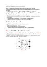
568 Chapter 8 Sequential Logic Design PracticesDOdevicesNOToperating at 25ºC but, dependingCOPYon the logic family, they could be for atypical part and nominal power-supply voltage, or they could be for a worst-casepart at worst-case supply voltage. “Maximum” values are generally valid overthe commercial operating range of voltage and temperature, except TTL values,DOwhichNOTare specified at 25ºC. Also noteCOPYthat the “maximum” values of t s , t h , t rec ,or t w are the maximum values of the minimum setup time, hold time, recoverytime, or pulse width that the specified part will exhibit.Different manufacturers may use slightly different definitions for the sametiming parameters, and they may specify different numbers for the same part. ADOgivenNOTmanufacturer may even use differentCOPYdefinitions for different families orpart numbers in the same family. Thus, all of the specifications in Table 8-1 aremerely representative; for exact numbers and their definitions, you must consultthe data sheet for the particular part and manufacturer.DO8.2NOTLatches and Flip-FlopsCOPY8.2.1 SSI Latches and Flip-FlopsSeveral different types of discrete latches and flip-flops are available as SSIparts. These devices are sometimes used in the design of state machines andDO“unstructured”NOTsequential circuits thatCOPYdon’t fall into the categories of shiftregisters, counters, and other sequential MSI functions presented later in this<strong>chapter</strong>. However, SSI latches and flip-flops have been eliminated to a largeextent in modern designs as their functions are embedded in PLDs and FPGAs.Nevertheless, a handful of these discrete building blocks still appear in manyDO NOT COPYdigital systems, so it’s important to be familiar with them.Figure 8-3 shows the pinouts for several SSI sequential devices. The only74x375latch in the figure is the 74x375, which contains four D latches, similar infunction to the “generic” D latches described in Section 7.2.4. Because of pinDOlimitations,NOTthe latches are arrangedCOPYin pairs with a common C control line foreach pair.74x74Among the devices in Figure 8-3, the most important is the 74x74, whichcontains two independent positive-edge-triggered D flip-flops with preset andclear inputs. We described the functional operation, timing, and internalDOstructureNOTof edge-triggered D flip-flopsCOPYin general, and the 74x74 in particular, inSection 7.2.5. Besides the 74x74’s use in “random” sequential circuits, fast74F74versions of the part, such as the 74F74 and 74ACT74, find application in74ACT74synchronizers for asynchronous input signals, as discussed in Section 8.9.74x109The 74x109 is a positive-edge-triggered J-K flip-flop with an active-low KDOinputNOT(named K or K_L). We discussedCOPYthe internal structure of the ’109 in74x112Section 7.2.10. Another J-K flip-flop is the 74x112, which has an active-lowclock input.Copyright © 1999 by John F. WakerlyCopying Prohibited
Section 8.2 Latches and Flip-Flops 569DO NOT COPY45474x7474x10974x11274x3752 PR 52 PR 63 PR 54D QJQJQ1,2C3411 1Q3CLKCLK1D2CLK637261QQK QK QDO NOT COPY5CLRCLRCLR7 2Q2D62Q1115123,4C119 3Q3D101011103Q74x7474x10974x1121315 4QDO12 PR 9NOT14 PR 1011COPYPR 94D14D QJQJQ4Q121311CLKCLKCLK8139127QK QK QCLRCLRCLRFigure 8-3131514DO NOT COPYPinouts for SSIlatches and flip-flops.*8.2.2 Switch DebouncingA common application of simple bistables and latches is switch debouncing.We’reDOall familiar with electricalNOTswitches from experience withCOPYlights, garbagedisposals, and other appliances. Switches connected to sources of constant logic0 and 1 are often used in digital systems to supply “user inputs.” However, indigital logic applications we must consider another aspect of switch operation,the time dimension. A simple make or break operation, which occurs instantlyas farDOas we slow-moving humansNOTare concerned, actually has severalCOPYphases thatare discernible by high-speed digital logic.Figure 8-4(a) shows how a single-pole, single-throw (SPST) switch mightbe used to generate a single logic input. A pull-up resistor provides a logic-1value when the switch is opened, and the switch contact is tied to ground toprovideDOa logic-1 value whenNOTthe switch is pushed.COPYAs shown in (b), it takes a while after a push for the wiper to hit the bottomcontact. Once it hits, it doesn’t stay there for long; it bounces a few times beforefinally settling. The result is that several transitions are seen on the SW_L andDSW logic signals for each single switch push. This behavior is called contact contact bouncebounce.DOTypical switches bounceNOTfor 10–20 ms, a very long timeCOPYcompared to theswitching speeds of logic gates.Contact bounce may or may not be a problem, depending on the switchapplication. For example, some computers have configuration informationspecifiedDOby small switches,NOTcalled DIP switches because theyCOPYare the same size DIP switchas a dual in-line package (DIP). Since DIP switches are normally changed onlywhen the computer is inactive, there’s no problem. Contact bounce is a problem* Throughout this book, optional sections are marked with an asterisk.Copyright © 1999 by John F. WakerlyCopying Prohibited