chapter 8.pdf
chapter 8.pdf
chapter 8.pdf

You also want an ePaper? Increase the reach of your titles
YUMPU automatically turns print PDFs into web optimized ePapers that Google loves.
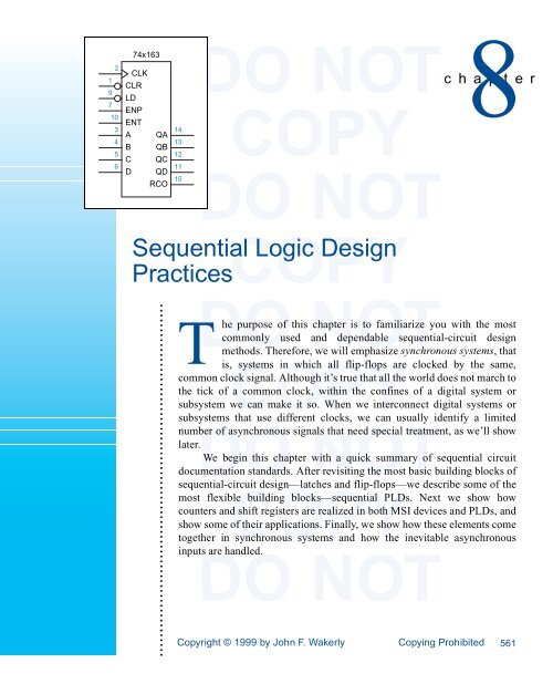
219710345674x163CLKCLRLDENPENTABCDQAQBQCQDRCO1413121115DO NOTCOPYDO NOT8c h a p t e rCOPYSequential Logic DesignPractices• • • • • • • • • • • • • • • • • • • • • • • • • • • • • • • • • • • • • • • • • • • • • • • • • • • • • • • • • • • • • • • • • • • • • • • •TDONOTCOPYDO NOTCOPYDO NOThe purpose of this <strong>chapter</strong> is to familiarize you with the mostcommonly used and dependable sequential-circuit designmethods. Therefore, we will emphasize synchronous systems, thatis, systems in which all flip-flops are clocked by the same,common clock signal. Although it’s true that all the world does not march tothe tick of a common clock, within the confines of a digital system orsubsystem we can make it so. When we interconnect digital systems orsubsystems that use different clocks, we can usually identify a limitednumber of asynchronous signals that need special treatment, as we’ll showlater.We begin this <strong>chapter</strong> with a quick summary of sequential circuitdocumentation standards. After revisiting the most basic building blocks ofsequential-circuit design—latches and flip-flops—we describe some of themost flexible building blocks—sequential PLDs. Next we show howcounters and shift registers are realized in both MSI devices and PLDs, andshow some of their applications. Finally, we show how these elements cometogether in synchronous systems and how the inevitable asynchronousinputs are handled.Copyright © 1999 by John F. WakerlyCopying Prohibited561
562 Chapter 8 Sequential Logic Design PracticesDO8.1NOTSequential Circuit DocumentationCOPYStandards8.1.1 General RequirementsBasic documentation standards in areas like signal naming, logic symbols, andschematic layout, which we introduced in Chapter 5, apply to digital systems asDOa wholeNOTand therefore to sequentialCOPYcircuits in particular. However, there areseveral ideas to highlight for system elements that are specifically “sequential”:• State-machine layout. Within a logic diagram, a collection of flip-flops andcombinational logic that forms a state machine should be drawn togetherDO NOTin a logical format on the sameCOPYpage, so the fact that it is a state machine isobvious. (You shouldn’t have to flip pages to find the feedback path!)• Cascaded elements. In a similar way, registers, counters, and shift registersthat use multiple ICs should have the ICs grouped together in the schematicso that the cascading structure is obvious.DO NOT COPY• Flip-flops. The symbols for individual sequential-circuit elements,especially flip-flops, should rigorously follow the appropriate drawingstandards, so that the type, function, and clocking behavior of the elementsare clear.DO•NOTState-machine descriptions. StateCOPYmachines should be described by statetables, state diagrams, transition lists, or text files in a state-machinedescription language such as ABEL or VHDL.• Timing diagrams. The documentation package for sequential circuitsDO NOTshould include timing diagramsCOPYthat show the general timing assumptionsand timing behavior of the circuit.• Timing specifications. A sequential circuit should be accompanied by aspecification of the timing requirements for proper internal operation (e.g.,maximum clock frequency), as well as the requirements for any externallyDO NOTsupplied inputs (e.g., setup- andCOPYhold-time requirements with respect to thesystem clock, minimum pulse widths, etc.).8.1.2 Logic SymbolsWe introduced traditional symbols for flip-flops in Section 7.2. Flip-flops areDOalwaysNOTdrawn as rectangular-shapedCOPYsymbols, and follow the same generalguidelines as other rectangular-shaped symbols—inputs on the left, outputs onthe right, bubbles for active levels, and so on. In addition, some specific guidelinesapply to flip-flop symbols:DO•NOTA dynamic indicator is placed onCOPYedge-triggered clock inputs.• A postponed-output indicator is placed on master/slave outputs that changeat the end interval during which the clock is asserted.• Asynchronous preset and clear inputs may be shown at the top and bottomof a flip-flop symbol—preset at the top and clear at the bottom.Copyright © 1999 by John F. WakerlyCopying Prohibited
Section 8.1 Sequential Circuit Documentation Standards 563DOThe logic symbols forNOTlarger-scale sequential elements,COPYsuch as thecounters and shift register described later in this <strong>chapter</strong>, are generally drawnwith all inputs, including presets and clears, on the left, and all outputs on theright. Bidirectional signals may be drawn on the left or the right, whichever isconvenient.DO NOT COPYLike individual flip-flops, larger-scale sequential elements use a dynamicindicator to indicate edge-triggered clock inputs. In “traditional” symbols, thenames of the inputs and outputs give a clue of their function, but they are sometimesambiguous. For example, two elements described later in this <strong>chapter</strong>, the74x161DOand 74x163 4-bit counters,NOThave exactly the same traditionalCOPYsymbol,even though the behavior of their CLR inputs is completely different.IEEE STANDARD IEEE standard symbols, which we show in Appendix A for all of the sequentialDOSYMBOLS elementsNOTin this <strong>chapter</strong>, have a rich set ofCOPYnotation that can provide an unambiguousdefinition of every signal’s function.8.1.3 State-Machine DescriptionsSoDOfar we have dealt with sixNOTdifferent representations of stateCOPYmachines:• Word descriptions• State tables• State diagramsDO NOT COPY• Transition lists• ABEL programs• VHDL programsYouDOmight think that havingNOTall these different ways to representCOPYstate machinesis a problem—too much for you to learn! Well, they’re not all that difficult tolearn, but there is a subtle problem here.Consider a similar problem in programming, where high-level “pseudocode”or perhaps a flowchart might be used to document how a program works.TheDOpseudo-code may expressNOTthe programmer’s intentions veryCOPYwell, but errors,misinterpretations, and typos can occur when the pseudo-code is translated intoreal code. In any creative process, inconsistencies can occur when there aremultiple representations of how things work.The same kind of inconsistencies can occur in state-machine design. A inconsistentlogicDOdesigner may documentNOTa machine’s desired behavior withCOPYa 100%-correct state-machinehand-drawn state diagram, but you can make mistakes translating the diagram representationsinto a program, and there are lots of opportunities to mess up if you have to“turning the crank” manually to translate the state diagram into a state table,transition table, excitation equations, and logic diagram.Copyright © 1999 by John F. WakerlyCopying Prohibited
564 Chapter 8 Sequential Logic Design PracticesDO NOTThe solution to this problem isCOPYsimilar to the one adopted by programmerswho write self-documenting code using a high-level language. The key is toselect a representation that is both expressive of the designer’s intentions andthat can be translated into a physical realization using an error-free, automatedDOprocess.NOT(You don’t hear many programmersCOPYscreaming “Compiler bug!” whentheir programs don’t work the first time.)The best solution (for now, at least) is to write state-machine “programs”directly in a high-level state-machine description language like ABEL orVHDL, and to avoid alternate representations, other than general, summaryDOwordNOTdescriptions. Languages like ABELCOPYand VHDL are easily readable andallow automatic conversion of the description into a PLD-, FPGA-, or ASICbasedrealization. Some CAD tools allow state machines to be specified andsynthesized using state diagrams, or even using sample timing diagrams, butthese can often lead to ambiguities and unanticipated results. Thus, we’ll useDOABEL/VHDLNOTapproach exclusively forCOPYthe rest of this book.8.1.4 Timing Diagrams and SpecificationsWe showed many examples of timing diagrams in Chapters 5 and 7. In thedesign of synchronous systems, most timing diagrams show the relationshipDObetweenNOTthe clock and various input,COPYoutput, and internal signals.Figure 8-1 shows a fairly typical timing diagram that specifies the requirementsand characteristics of input and output signals in a synchronous circuit.The first line shows the system clock and its nominal timing parameters. Theremaining lines show a range of delays for other signals.DO NOT COPYFor example, the second line shows that flip-flops change their outputs atsome time between the rising edge of CLOCK and time t ffpd afterward. Externalcircuits that sample these signals should not do so while they are changing. Thetiming diagram is drawn as if the minimum value of tDO NOT COPYffpd is zero; a completeFigure 8-1CLOCKA detailed timingtDO NOTH tdiagram showingpropagation delaysCOPYLt clkflip-flopand setup and holdoutputstimes with respect tot ffpdthe clock.combinationaloutputsDO NOTt combCOPYflip-flopinputst setupsetup-time marginCopyright © 1999 by John F. Wakerlyt holdCopying Prohibited
Section 8.1 Sequential Circuit Documentation Standards 565documentationDOpackage wouldNOTinclude a timing table indicatingCOPYthe actualminimum, typical, and maximum values of t ffpd and all other timing parameters.The third line of the timing diagram shows the additional time, t comb ,required for the flip-flop output changes to propagate through combinationallogicDOelements, such as flip-flopNOTexcitation logic. The excitationCOPYinputs of flipflopsand other clocked devices require a setup time of t setup , as shown in thefourth line. For proper circuit operation we must have t clk − t ffpd − t comb > t setup .Timing margins indicate how much “worse than worst-case” the individual timing margincomponents of a circuit can be without causing the circuit to fail. Well-designedsystemsDOhave positive, nonzeroNOTtiming margins to allow for unexpectedCOPYcircumstances(marginal components, brown-outs, engineering errors, etc.) and clockskew (Section 8.8.1).The value tDOclk − t ffpd(max) − tNOTcomb(max) − t setup is called the setup-time margin; setup-time marginif this is negative, the circuit won’t work. Note that maximum propagation delaysare used to calculate setup-time margin. Another timing marginCOPYinvolves thehold-time requirement t hold ; the sum of the minimum values of t ffpd and t combmust be greater than t hold , and the hold-time margin is t ffpd(min) + t comb(min) − t hold . hold-time marginThe timing diagram in Figure 8-1 does not show the timing differencesbetween different flip-flop inputs or combinational-logic signals, even thoughsuchDOdifferences exist in mostNOTcircuits. For example, one flip-flop’sCOPYQ outputmay be connected directly to another flip-flop’s D input, so that t comb forthat path is zero, while another’s may go the ripple-carry path of a 32-bitadder before reaching a flip-flop input. When proper synchronous designmethodology is used, these relative timings are not critical, since none of theseDO NOT COPYsignals affect the state of the circuit until a clock edge occurs. You merely haveto find the longest delay path in one clock period to determine whether thecircuit will work. However, you may have to analyze several different paths inorder to find the worst-case one.DOAnother, perhaps moreNOTcommon, type of timing diagramCOPYshows onlyfunctional behavior and is not concerned with actual delay amounts; an exampleis shown in Figure 8-2. Here, the clock is “perfect.” Whether to show signalchanges as vertical or slanted lines is strictly a matter of personal taste in this andall other timing diagrams, unless rise and fall times must be explicitly indicated.ClockDOtransitions are shownNOTas vertical lines in this and other figuresCOPYin keepingwith the idea that the clock is a “perfect” reference signal.CLOCKFigure 8-2DO NOT COPYFunctional timing of aSYNC_Lsynchronous circuit.SIG1DBUS DATA1 DATA2Copyright © 1999 by John F. WakerlyCopying Prohibited
566 Chapter 8 Sequential Logic Design PracticesDO NOT COPYNOTHING’S In reality, there’s no such thing as a perfect clock signal. One imperfection that mostPERFECT designers of high-speed digital circuits have to deal with is “clock skew.” As weshow in Section 8.8.1, a given clock edge arrives at different circuit inputs at differentDO NOTtimes because of differences in wiringCOPYdelays, loading, and other effects.Another imperfection, a bit beyond the scope of this text, is “clock jitter.” A10-MHz clock does not have a period of exactly 100 ns on every cycle—it may be100.05 ns in one cycle, and 99.95 ns in the next. This is not a big deal in such a slowcircuit, but in a 500-MHz circuit, the same 0.1 ns of jitter eats up 5% of the 2-nsDOtimingNOTbudget. And the jitter in some clockCOPYsources is even higher!The other signals in Figure 8-2 may be flip-flop outputs, combinationaloutputs, or flip-flop inputs. Shading is used to indicate “don’t-care” signalvalues; cross-hatching as in Figure 8-1 on the preceding page could be usedDO NOT COPYinstead. All of the signals are shown to change immediately after the clock edge.In reality, the outputs change sometime later, and inputs may change just barelybefore the next clock edge. However, “lining up” everything on the clock edgeallows the timing diagram to display more clearly which functions areDOperformedNOTduring each clock period.COPYSignals that are lined up with the clock aresimply understood to change sometime after the clock edge, with timing thatmeets the setup- and hold-time requirements of the circuit. Many timingdiagrams of this type appear in this <strong>chapter</strong>.Table 8-1 shows manufacturer’s timing parameters for commonly usedDOflip-flops,NOTregisters, and latches in CMOSCOPYand TTL. “Typical” values are forTable 8-1 Propagation delay in ns of selected CMOS flip-flops, registers, and latches.74HCT 74AHCT 74FCT 74LSPart Parameter Typ. Max. Typ. Max. Min. Max. Typ. Max.DO NOT COPY’74 t pd , CLK↑ to Q or Q 35 44 6.3 10 25 40t pd , PR↓ or CLR↓ to Q or Q 40 50 8.1 13 25 40tDOs , D to CLK↑ 12 15 5 20t h , D from CLK↑ 3 3 0 5t rec , CLK↑ from PR↑ orNOTCLR↑ 6 8COPY3.5t w , CLK low or high 18 23 5 25t w , PR or CLR low 16 20 5 25’174 tDOpd , CLK↑ to Q 40 50 6.3 10 21 30t pd , CLR↓ to Q 44 55 8.1 13 23 35t s , D to CLK↑NOT16 20COPY5 20t h , D from CLK↑ 5 5 0 5t rec , CLK↑ from CLR↑ 12 15 3.5 25t w , CLK low or high 20 25 5 20t w , CLR low 25 31 5 20Copyright © 1999 by John F. WakerlyCopying Prohibited
568 Chapter 8 Sequential Logic Design PracticesDOdevicesNOToperating at 25ºC but, dependingCOPYon the logic family, they could be for atypical part and nominal power-supply voltage, or they could be for a worst-casepart at worst-case supply voltage. “Maximum” values are generally valid overthe commercial operating range of voltage and temperature, except TTL values,DOwhichNOTare specified at 25ºC. Also noteCOPYthat the “maximum” values of t s , t h , t rec ,or t w are the maximum values of the minimum setup time, hold time, recoverytime, or pulse width that the specified part will exhibit.Different manufacturers may use slightly different definitions for the sametiming parameters, and they may specify different numbers for the same part. ADOgivenNOTmanufacturer may even use differentCOPYdefinitions for different families orpart numbers in the same family. Thus, all of the specifications in Table 8-1 aremerely representative; for exact numbers and their definitions, you must consultthe data sheet for the particular part and manufacturer.DO8.2NOTLatches and Flip-FlopsCOPY8.2.1 SSI Latches and Flip-FlopsSeveral different types of discrete latches and flip-flops are available as SSIparts. These devices are sometimes used in the design of state machines andDO“unstructured”NOTsequential circuits thatCOPYdon’t fall into the categories of shiftregisters, counters, and other sequential MSI functions presented later in this<strong>chapter</strong>. However, SSI latches and flip-flops have been eliminated to a largeextent in modern designs as their functions are embedded in PLDs and FPGAs.Nevertheless, a handful of these discrete building blocks still appear in manyDO NOT COPYdigital systems, so it’s important to be familiar with them.Figure 8-3 shows the pinouts for several SSI sequential devices. The only74x375latch in the figure is the 74x375, which contains four D latches, similar infunction to the “generic” D latches described in Section 7.2.4. Because of pinDOlimitations,NOTthe latches are arrangedCOPYin pairs with a common C control line foreach pair.74x74Among the devices in Figure 8-3, the most important is the 74x74, whichcontains two independent positive-edge-triggered D flip-flops with preset andclear inputs. We described the functional operation, timing, and internalDOstructureNOTof edge-triggered D flip-flopsCOPYin general, and the 74x74 in particular, inSection 7.2.5. Besides the 74x74’s use in “random” sequential circuits, fast74F74versions of the part, such as the 74F74 and 74ACT74, find application in74ACT74synchronizers for asynchronous input signals, as discussed in Section 8.9.74x109The 74x109 is a positive-edge-triggered J-K flip-flop with an active-low KDOinputNOT(named K or K_L). We discussedCOPYthe internal structure of the ’109 in74x112Section 7.2.10. Another J-K flip-flop is the 74x112, which has an active-lowclock input.Copyright © 1999 by John F. WakerlyCopying Prohibited
Section 8.2 Latches and Flip-Flops 569DO NOT COPY45474x7474x10974x11274x3752 PR 52 PR 63 PR 54D QJQJQ1,2C3411 1Q3CLKCLK1D2CLK637261QQK QK QDO NOT COPY5CLRCLRCLR7 2Q2D62Q1115123,4C119 3Q3D101011103Q74x7474x10974x1121315 4QDO12 PR 9NOT14 PR 1011COPYPR 94D14D QJQJQ4Q121311CLKCLKCLK8139127QK QK QCLRCLRCLRFigure 8-3131514DO NOT COPYPinouts for SSIlatches and flip-flops.*8.2.2 Switch DebouncingA common application of simple bistables and latches is switch debouncing.We’reDOall familiar with electricalNOTswitches from experience withCOPYlights, garbagedisposals, and other appliances. Switches connected to sources of constant logic0 and 1 are often used in digital systems to supply “user inputs.” However, indigital logic applications we must consider another aspect of switch operation,the time dimension. A simple make or break operation, which occurs instantlyas farDOas we slow-moving humansNOTare concerned, actually has severalCOPYphases thatare discernible by high-speed digital logic.Figure 8-4(a) shows how a single-pole, single-throw (SPST) switch mightbe used to generate a single logic input. A pull-up resistor provides a logic-1value when the switch is opened, and the switch contact is tied to ground toprovideDOa logic-1 value whenNOTthe switch is pushed.COPYAs shown in (b), it takes a while after a push for the wiper to hit the bottomcontact. Once it hits, it doesn’t stay there for long; it bounces a few times beforefinally settling. The result is that several transitions are seen on the SW_L andDSW logic signals for each single switch push. This behavior is called contact contact bouncebounce.DOTypical switches bounceNOTfor 10–20 ms, a very long timeCOPYcompared to theswitching speeds of logic gates.Contact bounce may or may not be a problem, depending on the switchapplication. For example, some computers have configuration informationspecifiedDOby small switches,NOTcalled DIP switches because theyCOPYare the same size DIP switchas a dual in-line package (DIP). Since DIP switches are normally changed onlywhen the computer is inactive, there’s no problem. Contact bounce is a problem* Throughout this book, optional sections are marked with an asterisk.Copyright © 1999 by John F. WakerlyCopying Prohibited
570 Chapter 8 Sequential Logic Design PracticesDO NOT COPY+5V(a)push74LS04DO NOTSW_LCOPYDSWfirst contact bouncepush(b)DO NOT COPY+5VSW_LGNDFigure 8-4Switch input without1DO NOTDSWdebouncing.COPY0if a switch is being used to count or signal some event (e.g., laps in a race). Thenwe must provide a circuit (or, in microprocessor-based systems, software) todebouncedebounce the switch—to provide just one signal change or pulse for eachDOexternalNOTevent.COPY*8.2.3 The Simplest Switch DebouncerSwitch debouncing is a good application for the simplest sequential circuit, thebistable element of Section 7.1, which can be used as shown in Figure 8-5. ThisDOcircuitNOTuses a single-pole, double-throwCOPY(SPDT) switch. The switch contacts andwiper have a “break before make” behavior, so the wiper terminal is “floating”at some time halfway through the switch depression. iBefore the button is pushed, the top contact holds SW at 0 V, a valid logic0, and the top inverter produces a logic 1 onDO NOT COPYSW_L and on the bottom contact.When the button is pushed and contact is broken, feedback in the bistable holdsSW at V OL ( ≤ 0.5 V for LS-TTL), still a valid logic 0.Next, when the wiper hits the bottom contact, the circuit operates quiteunconventionally for a moment. The top inverter in the bistable is trying toDOmaintainNOTa logic 1 on the SW_L signal;COPYthe top transistor in its totem-pole outputis “on” and connecting SW_L through a small resistance to +5 V. Suddenly,the switch contact makes a metallic connection of SW_L to ground, 0.0 V. Notsurprisingly, the switch contact wins.A short time later (30 ns for the 74LS04), the forced logic 0 on SW_LDOpropagatesNOTthrough the two invertersCOPYof the bistable, so that the top inverter givesup its vain attempt to drive a 1, and instead drives a logic 0 onto SW_L. At thispoint, the top inverter output is no longer shorted to ground, and feedback in thebistable maintains the logic 0 on SW_L even if the wiper bounces off the bottomcontact, as it does. (It does not bounce far enough to touch the top contact again.)Copyright © 1999 by John F. WakerlyCopying Prohibited
Section 8.2 Latches and Flip-Flops 571DO NOT COPY74LS0474LS04push SWSW_LDSW(a)DO NOTSW_LSWCOPYVDO NOTOH pushSWV OLCOPYGNDfirst contact(b)bounceV OHSW_LVDOOLFigure 8-5GNDSwitch input usingNOT COPY1a bistable forDSW0debouncingAdvantages of this circuit compared to other debouncing approaches arethatDOit has a low chip countNOT(one-third of a 74LS04), no pull-upCOPYresistors arerequired, and both polarities of the input signal (active-high and active-low)are produced. In situations where momentarily shorting gate outputs must beavoided, a similar circuit can be designed using a S-R latch and pull-up resistors,as suggested in Figure 8-6.DO NOT COPY+5 VFigure 8-6Switch input using74LS00an S-R latch forSWU_LDO NOTDSW_L debouncing.COPYpush+5 VDSWSWD_LDO NOT COPYWHERE WIMPY The circuit in Figure 8-5, while elegant, should not be used with high-speed CMOSWORKS WELL devices, like the 74ACT04, whose outputs are capable of sourcing large amounts ofDOcurrentNOTin the HIGH state. While shortingCOPYsuch outputs to ground momentarily willnot cause any damage, it will generate a noise pulse on power and ground signals thatmay trigger improper operation of the circuit elsewhere. The debouncing circuit inthe figure works well with wimpy logic families like HCT and LS-TTL.Copyright © 1999 by John F. WakerlyCopying Prohibited
572 Chapter 8 Sequential Logic Design PracticesDO*8.2.4NOTBus Holder CircuitCOPYIn Sections 3.7.3 and 5.6 we described three-state outputs and how they are tiedtogether to create three-state buses. At any time, at most one output can drive thebus; sometimes, no output is driving the bus, and the bus is “floating.” WhenDOhigh-speedNOTCMOS inputs are connectedCOPYto a bus that is left floating for a longtime (in the fastest circuits, more than a clock tick or two), bad things canhappen. In particular, noise, crosstalk, and other effects can drive the highimpedancefloating bus signals to a voltage level near the CMOS devices’ inputswitching threshold, which in turn allows excessive current to flow in the deviceDOoutputs.NOTFor this reason, it is desirableCOPYand customary to provide pull-up resistorsthat quickly pull a floating bus to a valid HIGH logic level.Pull-up resistors aren’t all goodness—they cost money and they occupyvaluable printed-circuit-board real estate. A big problem they have in very highspeedcircuits is the choice of resistance value. If the resistance is too high, whenDOa busNOTgoes from LOW to floating, theCOPYtransition from LOW to pulled-up (HIGH)will be slow due to the high RC time constant, and input levels may spend toomuch time near the switching threshold. If the pull-up resistance is too low,devices trying to pull the bus LOW will have to sink too much current.The solution to this problem is to eliminate pull-up resistors in favor of anDO NOT COPYbus holder circuit active bus holder circuit, shown in Figure 8-7. This is nothing but a bistable witha resistor R in one leg of the feedback loop. The bus holder’s INOUT signal isconnected to the three-state bus line which is to be held. When the three-stateoutput currently driving the line LOW or HIGH changes to floating, the busDOholder’sNOTright-hand inverter holds theCOPYline in its current state. When a three-stateoutput tries to change the line from LOW to HIGH or vice versa, it must source orsink a small amount of additional current through R to overcome the bus holder.This additional current flow persists only for the short time that it takes for thebistable to flip into its other stable state.DO NOTThe choice of the value of R in theCOPYbus holder is a compromise between lowoverride current (high R) and good noise immunity on the held bus line (low R).A typical example, bus holder circuits in the 3.3-V CMOS LVC family specify amaximum override current of 500 µA, implying R ≈ 3.3 / 0.0005 = 6.6KΩ.Bus holder circuits are often built into another MSI device, such as an octalDOCMOSNOTbus driver or transceiver. TheyCOPYrequire no extra pins and require verylittle chip area, so they are essentially free. And there’s no real problem in havingmultiple (n) bus holders on the same signal line, as long as the bus drivers canprovide n times the override current for a few nanoseconds during switching.Note that bus holders normally are not effective on buses that have TTL inputsDOattachedNOTto them (see Exercise 8.14).COPYFigure 8-7Bus holder circuit.RINOUTCopyright © 1999 by John F. WakerlyCopying Prohibited
Section 8.2 Latches and Flip-Flops 5738.2.5DOMultibit RegistersNOTand LatchesCOPYA collection of two or more D flip-flops with a common clock input is called aregister. Registers are often used to store a collection of related bits, such as a registerbyte of data in a computer. However, a single register can also be used to storeunrelatedDObits of data or controlNOTinformation; the only real constraintCOPYis that allof the bits are stored using the same clock signal.Figure 8-8 shows the logic diagram and logic symbol for a commonly usedMSI register, the 74x175. The 74x175 contains four edge-triggered D flip-flops 74x175with a common clock and asynchronous clear inputs. It provides both activehighDOand active-low outputs atNOTthe external pins of the device.COPYThe individual flip-flops in a ’175 are negative-edge triggered, as indicatedby the inversion bubbles on their CLK inputs. However, the circuit also containsan inverter that makes the flip-flops positive-edge triggered with respect to thedevice’s external CLK input pin. The common, active-low, clear signal (CLR_L)is connectedDOto the asynchronousNOTclear inputs of all four flip-flops.COPYBoth CLK andCLR_L are buffered before fanning out to the four flip-flops, so that a devicedriving one of these inputs sees only one unit load instead of four. This isespecially important if a common clock or clear signal must drive many suchregisters.DO NOT COPY(4)(2)1DD Q1QFigure 8-8(3)CLK Q1Q_LThe 74x175 4-bit register:DO NOT(a)COPY(a) logic diagram, includingCLRpin numbers for a standard16-pin dual in-line package;(b) traditional logic symbol.(5)(7)2DD Q2Q(6)DO NOTCLK Q2Q_LCOPYCLR74x175(b) 9CLK(12)(10)13DD Q3QCLRDO NOT COPY2(11)4 1QCLK Q3Q_L1D31QCLR75 2Q2D62Q1012 3Q3D11DO(13)NOT(15)4DCOPYD Q4Q3Q15(14)13 4Q(9)CLK Q4Q_L4D14CLK4QCLR(1)CLR_LCopyright © 1999 by John F. WakerlyCopying Prohibited
574 Chapter 8 Sequential Logic Design PracticesDO NOT COPY74x174The logic symbol for the 74x174, 6-bit register is shown in Figure 8-9. The9internal structure of this device is similar to the 74x175’s, is similar, except thatCLK1it eliminates the active-low outputs and provides two more flip-flops instead.CLRMany digital systems, including computers, telecommunications devices,321D 1Q4DOandNOTstereo equipment, process informationCOPY8, 16, or 32 bits at a time; as a result,2D 2Q 56ICs that handle eight bits are very popular. One such MSI IC is the 74x374 octal3D 3Q 71110 edge-triggered D flip-flop, also known simply as an 8-bit register. (Once again,4D 4Q13“octal” means that the device has eight sections.)5D 5Q 121415As shown in Figure 8-10, the 74x374 contains eight edge-triggered D flipflops6D 6QDO NOTthat all sample their inputs andCOPYchange their outputs on the rising edge of aFigure 8-9 common CLK input. Each flip-flop output drives a three-state buffer that in turnLogic symbol for the drives an active-high output. All of the three-state buffers are enabled by a74x174 6-bit register.(1)OE_LDO NOT COPY(a)(3)1DD(2)CLK QFigure 8-101QThe 74x374 8-bit register:(a)DOlogic diagram, including pin(4)NOT2DCOPYDnumbers for a standard 20-pin(5)CLK Q2Qdual in-line package;(b) traditional logic symbol.(7)3DD(6)DO NOT COPYCLK Q3Q(8)4DD(b)(9)CLK Q4Q74x374DO NOT COPY11(13)CLK5DD1(12)OECLK Q5Q321D 1Q42D 2Q 5(14)DO73DNOT3Q 6 6DDCOPY(15)89CLK Q6Q4D 4Q135D 5Q 12(17)14156D 6Q7DD17 16(16)7D 7QCLK Q7Q18 19DO8DNOT8QCOPY(18)8DD(19)CLK Q8Q(11)CLKCopyright © 1999 by John F. WakerlyCopying Prohibited
Section 8.2 Latches and Flip-Flops 575common,DOactive-lowNOT COPYOE_L (output enable) input. As in the other registers thatwe’ve studied, the control inputs (CLK and OE_L) are buffered so that theypresent only one unit load to a device that drives them.One variation of the 74x374 is the 74x373, whose symbol is shown inFigureDO8-11. The ’373 uses DNOTlatches instead of edge-triggeredCOPYflip-flops. Therefore,its outputs follow the corresponding inputs whenever C is asserted, andlatch the last input values when C is negated. Another variation is the 74x273,shown in Figure 8-12. This octal register has non-three-state outputs and noOE_L input; instead it uses pin 1 for an asynchronous clear input CLR_L.DOThe 74x377, whose symbolNOTis shown in Figure 8-13(a),COPYis an edgetriggeredregister like the ’374, but it does not have three-state outputs. Instead,pin 1 is used as an active-low clock enable input EN_L. If EN_L is asserted(LOW) at the rising edge of the clock, then the flip-flops are loaded from the datainputs; otherwise, they retain their present values, as shown logically in (b).DO NOT COPY74x37374x273Figure 8-11Figure 8-121111CLogic symbol for theCLogic symbol for the11OE74x373 8-bit latch.CLR74x273 8-bit register.3232DO1D 1QNOT COPY1D 1Q42D 2Q 542D 2Q 573D 3Q 6 73D 3Q 689894D 4Q4D 4Q135D 5Q 12135D 5Q 12141514156D 6Q6D 6QDO NOT COPY17 1617 167D 7Q7D 7Q18 1918 198D 8Q8D 8QFigure 8-13 The 74x377 8-bit register with gated clock:DO(a) logic symbol;NOT(b) logical behavior of one bit.COPY(a)(b)74x37711CLK1DOENNOT COPY(19)32D Q 8Q1D 1Q4(18)CK2D 2Q 58D73D 3Q 6894D 4Q13DO5D 5Q 12NOT COPY(1)1415 EN_L6D 6Q17 167D 7Q18 19(11)8D 8QCLKCopyright © 1999 by John F. WakerlyCopying Prohibited
576 Chapter 8 Sequential Logic Design PracticesDO NOTHigh pin-count surface-mountCOPYpackaging supports even wider registers,drivers, and transceivers. Most common are 16-bit devices, but there are alsodevices with 18 bits (for byte parity) and 32 bits. Also, the larger packages canoffer more control functions, such as clear, clock enable, multiple outputDOenables,NOTand even a choice of latchingCOPYvs. registered behavior all in one device.8.2.6 Registers and Latches in ABEL and PLDsAs we showed in Section 7.11, registers are very easy to specify in ABEL. Forexample, Table 7-33 on page 543 showed an ABEL program for an 8-bit registerDOwithNOTenable. Obviously, ABEL allowsCOPYthe functions performed at the D inputs ofregister to be customized in almost any way desired, limited only by the numberof inputs and product terms in the targeted PLD. We describe sequential PLDsin Section 8.3.With most sequential PLDs, few if any customizations can be applied to aDOregister’sNOTclock input (e.g, polarity choice)COPYor to the asynchronous inputs (e.g.,different preset conditions for different bits). However, ABEL does provideappropriate syntax to apply these customizations in devices that support them, asdescribed in Section 7.11.1.Very few PLDs have latches built in; edge-triggered registers are muchDOmoreNOTcommon, and generally more useful.COPYHowever, you can also synthesize alatch using combinational logic and feedback. For example, the excitation equationfor an S-R latch isQ∗ = S + R′⋅QDOThus,NOTyou could build an S-R latchCOPYusing one combinational output of a PLD,using the ABEL equation “Q = S # !R & Q.” Furthermore, the S and R signalsabove could be replaced with more complex logic functions of the PLD’s inputs,limited only by the availability of product terms (seven per output in a 16V8Cor 16L8) to realize the final excitation equation. The feedback loop can beDOcreatedNOTonly when Q is assigned to aCOPYbidirectional pin (in a 16V8C or 16L8, pinsIO2–IO7, not O1 or O8). Also, the output pin must be continuously outputenabled;otherwise, the feedback loop would be broken and the latch’s state lost.Probably the handiest latch to build out of a combinational PLD is a Dlatch. The basic excitation equation for a D latch isDO NOT COPYQ∗ = C ⋅ D + C′⋅QHowever, we showed in Section 7.10.1 that this equation contains a static hazard,and the corresponding circuit does not latch data reliably. To build a reliableD latch, we must include a consensus term in the excitation equation:DO NOTQ∗ = C ⋅ DCOPY+ C′⋅Q + D ⋅ QThe D input in this equation may be replaced with a more complicated expression,but the equation’s structure remains the same:Q∗ = C ⋅ expression + C′⋅Q + expression ⋅ QCopyright © 1999 by John F. WakerlyCopying Prohibited
Section 8.2 Latches and Flip-Flops 577DO NOT COPYABUS ADDR1 ADDR2AVALIDDOREAD_LNOT COPYROMCS_LFigure 8-14Timing diagram for aDBUS DATA1 DATA2 microprocessor readDOfrom ROMNOTfrom a different deviceCOPYoperation.It is also possible to use a more complex expression for the C input, as weshowed in Section 7.10.1. In any case, it is very important for the consensus termto be included in the PLD realization. The compiler can work against you in thiscase,DOsince its minimizationNOTstep will find that the consensusCOPYterm is redundantand remove it.Some versions of the ABEL compiler let you prevent elimination ofconsensus terms by including a keyword “retain” in the property list of the retain propertyistype declaration for any output which is not to be minimized. In otherDO NOT COPYversions, your only choice is to turn off minimization for the entire design.Probably the most common use of a PLD-based latch is to simultaneouslydecode and latch addresses in order to select memory and I/O devices in microprocessorsystems. Figure 8-14 is a timing diagram for this function in a typicalsystem.DOThe microprocessorNOTselects a device and a location withinCOPYthe device byplacing an address on its address bus (ABUS) and asserting an “address valid”signal (AVALID). A short time later, it asserts a read signal (READ_L), and theselected device responds by placing data on the data bus (DBUS).Notice that the address does not stay valid on ABUS for the entire operation.DOThe microprocessor busNOTprotocol expects the address toCOPYbe latched usingAVALID as an enable, then decoded, as shown in Figure 8-15. The decoderselects different devices to be enabled or “chip-selected” according to the highorderbits of the address (the 12 high-order bits in this example). The low-orderbits are used to address individual locations of a selected device.DO NOT COPY32-bit latchdecoderto individual Figure 8-15device MicroprocessorQ[31:20]chip-select address latching andinputsDO NOT COPYdecoding circuit.ABUS[31:0] D[31:0]to deviceQ[19:0]addressAVALID GinputsCopyright © 1999 by John F. WakerlyCopying Prohibited
578 Chapter 8 Sequential Logic Design PracticesDO NOT COPYWHY A LATCH? The microprocessor bus protocol in Figure 8-14 raises several questions:• Why not keep the address valid on ABUS for the entire operation? In a realsystem using this protocol, the functions of ABUS and DBUS are combinedDO NOT(multiplexed) onto one three-state busCOPYto save pins and wires.• Why not use AVALID as the clock input to a positive-edge-triggered register tocapture the address? There isn’t enough setup time; in a real system, the addressmay first be valid at or slightly after the rising edge of AVALID.• OK, so why not use AVALID to clock a negative-edge-triggered register? ThisDO NOTworks, but the latched outputs are availableCOPYsooner; valid values on ABUS flowthrough a latch immediately, without waiting for the falling clock edge. Thisrelaxes the access-time requirements of memories and other devices driven bythe latched outputs.DO NOT COPYUsing a PLD, the latching and decoding functions for the high-order bitscan be combined into a single device, yielding the block diagram in Figure 8-16.Compared with Figure 8-15, the “latching decoder” saves devices and pins, andmay produce a valid chip-select output more quickly (see Exercise 8.1).DO NOTTable 8-2 is an ABEL programCOPYfor the latching decoder. Since it operateson only the high-order bits ABUS[31..20], it can decode addresses only in1-Mbyte or larger chunks (2 20 = 1M). A read-only memory (ROM) is locatedin the highest 1-Mbyte chunk, addresses 0xfff00000–0xffffffff, and isselected by ROMCS. Three 16-Mbyte banks of read/write memory (RAM) areDO NOT COPYlocated at lower addresses, starting at addresses 0x00000000, 0x00100000, and0x00200000, respectively. Notice how don’t-cares are used in the definitions ofthe RAM bank address ranges to decode a chunk larger than 1 Mbyte. Otherapproaches to these definitions are also possible (e.g., see Exercise 8.2).DO NOTThe equations in Table 8-2 forCOPYthe chip-select outputs follow the D-latchtemplate that we gave on page 576. The expressions that select a device, such as“ABUS==ROM,” each generate a single product term, and each equation generatesthree product terms. Notice the use of the “retain” property in the pin declarationsto prevent the compiler from optimizing away the consensus terms.DO NOT COPYFigure 8-16latchingto individualUsing a combined ABUS[31:20]decoderdeviceaddress latching andchip-selectdecoding circuit.GinputsDO NOT20-bit latchCOPYABUS[19:0] D[19:0]to deviceQ[19:0]addressAVALID GinputsCopyright © 1999 by John F. WakerlyCopying Prohibited
Section 8.2 Latches and Flip-Flops 579DO NOT COPYmodule latchdecTable 8-2title 'Latching Microprocessor Address Decoder'ABEL programfor a latching" Inputsaddress decoder.AVALID, ABUS31..ABUS20pin;" LatchedDOand decoded outputsNOT COPYROMCS, RAMCS0, RAMCS1, RAMCS2 pin istype 'com,retain';ABUS = [ABUS31..ABUS20];ROM = ^hFFF;RAMBANK0DO= [0,0,0,0,0,0,0,0,.X.,.X.,.X.,.X.];NOT COPYRAMBANK1 = [0,0,0,0,0,0,0,1,.X.,.X.,.X.,.X.];RAMBANK2 = [0,0,0,0,0,0,1,0,.X.,.X.,.X.,.X.];equationsROMCSDO= AVALID & (ABUS==ROM)NOT# !AVALID & ROMCSCOPY# (ABUS==ROM) & ROMCS;RAMCS0 = AVALID & (ABUS==RAMBANK0) # !AVALID & RAMCS0# (ABUS==RAMBANK0) & RAMCS0;RAMCS1 = AVALID & (ABUS==RAMBANK1) # !AVALID & RAMCS1# (ABUS==RAMBANK1) & RAMCS1;RAMCS2DO= AVALID & (ABUS==RAMBANK2)NOT# !AVALID & RAMCS2COPY# (ABUS==RAMBANK2) & RAMCS2;end latchdecDO NOT COPYAfter seeing how easy it is to build S-R and D latches using combinationalPLDs, you might be tempted to go further and try to build an edge-triggered Dflip-flop. Although this is possible, it is expensive because an edge-triggeredflip-flop has four internal states and thus two feedback loops, consuming twoPLDDOoutputs. Furthermore, theNOTsetup and hold times and propagationCOPYdelays ofsuch a flip-flop would be quite poor compared to those of a discrete flip-flop inthe same technology. Finally, as we discussed in Section 7.10.6, the flow tablesof all edge-triggered flip-flops contain essential hazards, which can be maskedonly by controlling path delays, difficult in a PLD-based design.DO NOT COPY8.2.7 Registers and Latches in VHDLRegister and latch circuits can be specified using structural VHDL. For example,Table 8-3 is a structural VHDL program corresponding to the D latch circuit ofFigure 7-12 on page 443. However, writing structural programs is not really ourmotivationDOfor using VHDL;NOTour goal is to use behavioral programsCOPYto model theoperation of circuits more intuitively.Table 8-4 is a process-based behavioral architecture for the D latch thatrequires, in effect, just one line of code to describe the latch’s behavior. Note thatthe VHDL compiler “infers” a latch from this description—since the codeCopyright © 1999 by John F. WakerlyCopying Prohibited
580 Chapter 8 Sequential Logic Design PracticesDO NOT COPYTable 8-3 VHDL structural program for the D latch in Figure 7-12.library IEEE;use IEEE.std_logic_1164.all;entity Vdlatch isDOport (D, C: inNOTSTD_LOGIC;COPYQ, QN: buffer STD_LOGIC );end Vdlatch;architecture Vdlatch_s of Vdlatch issignal DN, SN, RN: STD_LOGIC;DOcomponent inv portNOT(I: in STD_LOGIC; O: outCOPYSTD_LOGIC ); end component;component nand2b port (I0, I1: in STD_LOGIC; O: buffer STD_LOGIC ); end component;beginU1: inv port map (D,DN);U2: nand2b port map (D,C,SN);DOU3: nand2b portNOTmap (C,DN,RN);COPYU4: nand2b port map (SN,QN,Q);U5: nand2b port map (Q,RN,QN);end Vdlatch_s;DO NOTTable 8-4 VHDL behavioral architectureCOPYfor a D latch.architecture Vdlatch_b of Vdlatch isbeginprocess(C, D, Q)DObeginNOT COPYif (C='1') then Q
Section 8.2 Latches and Flip-Flops 581DO NOT COPYBUFFS ‘N’ STUFF Note that in Table 8-3 we defined the type of Q and QN to be buffer rather than out,since these signals are used as inputs as well as outputs in the architecture definition.Then we had to define a special 2-input NAND gate nand2b with output type buffer,DOto avoidNOThaving a type mismatch (out vs.COPYbuffer) in the component instantiationsfor U4 and U5. Alternatively, we could have used internal signals to get around theproblem as shown in Table 8-5. As you know by now, VHDL has many differentways to express the same thing.DO NOT COPYTable 8-5 Alternative VHDL structural program for the D latch in Figure 7-12.library IEEE;use IEEE.std_logic_1164.all;entityDOVdlatch isNOT COPYport (D, C: in STD_LOGIC;Q, QN: out STD_LOGIC );end Vdlatch;architecture Vdlatch_s2 of Vdlatch issignal DN, SN, RN, IQ, IQN: STD_LOGIC;DO NOT COPYcomponent inv port (I: in STD_LOGIC; O: out STD_LOGIC ); end component;component nand2 port (I0, I1: in STD_LOGIC; O: out STD_LOGIC ); end component;beginU1: inv port map (D,DN);U2: nand2 port map (D,C,SN);U3:DOnand2 port map (C,DN,RN);NOT COPYU4: nand2 port map (SN,IQN,IQ);U5: nand2 port map (IQ,RN,IQN);Q
582 Chapter 8 Sequential Logic Design PracticesDO NOT COPYTable 8-7 VHDL model of a 74x74-like D flip-flop with preset and clear.library IEEE;use IEEE.std_logic_1164.all;DOentityNOTVdff74 isCOPYport (D, CLK, PR_L, CLR_L: in STD_LOGIC;Q, QN: out STD_LOGIC );end Vdff74;architecture Vdff74_b of Vdff74 issignal PR, CLR: STD_LOGIC;DObeginNOT COPYprocess(CLR_L, CLR, PR_L, PR, CLK)beginPR
Section 8.3 Sequential PLDs 583DOThe D-flip-flop modelNOTcan be augmented to include asynchronousCOPYinputsand a complemented output as in the 74x74 discrete flip-flop, as shown inTable 8-7. This more detailed functional model shows the non-complementarybehavior of the Q and QN outputs when preset and clear are asserted simultaneously.DOHowever, it doesNOTnot include timing behavior suchCOPYas propagationdelay and setup and hold times, which are beyond the scope of the VHDLcoverage in this book.Larger registers can of course be modeled by defining the data inputs andoutputs to be vectors, and additional functions can also be included. Forexample,DOTable 8-8 models aNOT16-bit register with three-state outputsCOPYand clockenable,output-enable, and clear inputs. An internal signal vector IQ is used tohold the flip-flop outputs, and three-state outputs are defined and enabled as inSection 5.6.4.DO NOT COPYSYNTHESIS In Table 8-8, the first elsif statement theoretically could have included all of theRESTRICTIONS conditions needed to assign D to IQ. That is, it could have read “elsif (CLK'event)and (CLK='1') and (CLKEN='1') then ...” instead of using a nested if statementDOto checkNOTCLKEN. However, it was writtenCOPYas shown for a very pragmatic reason.Only a subset of the VHDL language can be synthesized by the VHDLcompiler that was used to prepare this <strong>chapter</strong>; this is true of any VHDL compilertoday. In particular, use of the “event” attribute is limited to the form shown in theexample, and a few others, for detecting simple edge-triggered behavior. This getsmapped into edge-triggeredDO NOTD flip-flops during synthesis. The nested IF statementCOPYthat checks CLKEN in the example leads to the synthesis of multiplexer logic on theD inputs of these flip-flops.DO NOT COPY8.3 Sequential PLDs8.3.1 Bipolar Sequential PLDsThe PAL16R8, shown in Figure 8-17, is representative of the first generation of PAL16R8sequentialDOPLDs, which usedNOTbipolar (TTL) technology. ThisCOPYdevice has eightprimary inputs, eight outputs, and common clock and output-enable inputs, andfits in a 20-pin package.The PAL16R8’s AND-OR array is exactly the same as the one found in thePAL16L8 combinational PLD. However, the PAL16R8 has edge-triggered DDO NOT COPYflip-flops between the AND-OR array and its eight outputs, O1–O8. All of theflip-flops are connected to a common clock input, CLK, and change state on therising edge of the clock. Each flip-flop drives an output pin through a 3-statebuffer; the buffers have a common output-enable signal, OE_L. Notice that, likeCopyright © 1999 by John F. WakerlyCopying Prohibited
584 Chapter 8 Sequential Logic Design PracticesDOtheNOTcombinational output pins of a PAL16L8,COPYthe registered output pins of thePAL16R8 contain the complement of the signal produced by the AND-OR array.The possible inputs to the PAL16R8’s AND-OR array are eight primaryinputs (I1–I8) and the eight D flip-flop outputs. The connection from the D flipflopDO NOToutputs into the AND-OR arrayCOPYmakes it easy to design shift registers,counters, and general state machines. Unlike the PAL16L8’s combinationaloutputs, the PAL16R8’s D-flip-flop outputs are available to the AND-OR arraywhether or not the O1–O8 three-state drivers are enabled. Thus, the internal flipflopscan go to a next state that is a function of the current state even when theDOO1–O8NOToutputs are disabled.COPYMany applications require combinational as well as sequential PLDoutputs. The manufacturers of bipolar PLDs addressed this need by providing afew variants of the PAL16R8 that omitted the D flip-flops on some output pins,and instead provided input and output capability identical to that of theDOPAL16L8’sNOTbidirectional pins. For example,COPYFigure 8-18 is the logic diagram ofPAL16R6the PAL16R6, which has only six registered outputs. Two pins, IO1 and IO8, arebidirectional, serving both as inputs and as combinational outputs with separate3-state enables, just like the PAL16L8’s bidirectional pins. Thus, the possibleinputs to the PAL16R6’s AND-OR array are the eight primary inputs (I1–I8), theDOsixNOTD-flip-flop outputs, and the two bidirectionalCOPYpins (IO1, IO8).PAL16L8 PAL16R4Table 8-9 shows eight standard bipolar PLDs with differing numbers andPAL16R8types of inputs and outputs. All of the PAL16xx parts in the table use the samePAL20L8AND-OR array, where each output has eight AND gates, each with 16 variablesPAL20R4and their complements as possible inputs. The PAL20xx parts use a similarDO NOT COPYTable 8-9 Characteristics of standard bipolar PLDs.Inputs to AND arrayDO NOT COPYBidirectionalPart Package AND-gate Primary combinational Registered Combinationalnumber pins inputs inputs outputs outputs outputsPAL16L8 20 16 10 6 0 2DOPAL16R4NOT20 16 8COPY4 4 0PAL16R6 20 16 8 2 6 0PAL16R8 20 16 8 0 8 0PAL20L8 24 20 14 6 0 2DO NOT COPYPAL20R4 24 20 12 4 4 0PAL20R6 24 20 12 2 6 0PAL20R8 24 20 12 0 8 0Copyright © 1999 by John F. WakerlyCopying Prohibited
CLKI1I2I3I4I5I6I7I8Section 8.3 Sequential PLDs 585DO NOT COPY(1)0 1 2 3 4 5 6 7 8 9 1011 12131415 16171819 20212223 24252627 28293031012(19)3D Q4O15DO6NOT COPYQ7(2)8910(18)11D Q12O213DO NOT COPY14Q15(3)161718(17)19D Q20O3DO21NOT COPY22Q23(4)242526(16)27D Q28O4DO29NOT COPY30Q31(5)323334(15)35D QO5DO36NOT COPY3738Q39(6)404142(14)43D QDO44NOT COPYO64546Q47(7)484950(13)51DO NOT COPYD Q52O75354Q55(8)565758(13)DO59NOT COPYD Q60O86162Q63(9) (11)OE_LFigure 8-17 PAL16R8 logic diagram.Copyright © 1999 by John F. WakerlyCopying Prohibited
586 Chapter 8 Sequential Logic Design PracticesDO NOT COPY(1)CLK0 1 2 3 4 5 6 7 8 9 1011 12131415 16171819 20212223 24252627 282930310123(19)45DO6NOT COPY7(2)I18910(18)11D Q1213DO NOT COPY14Q15(3)I2161718(17)19D Q20DO21NOT COPY22Q23(4)I3242526(16)27D Q28DO29NOT COPY30Q31(5)I4323334(15)35D QDO36NOT COPY3738Q39(6)I5404142(14)43D QDO44NOT COPY4546Q47(7)I6484950(13)51DO NOT COPYD Q525354Q55(8)I7565758DO59NOT COPY(12)60616263(9) (11)I8Figure 8-18 PAL16R6 logic diagram.IO1O2O3O4O5O6O7IO8OE_LCopyright © 1999 by John F. WakerlyCopying Prohibited
Section 8.3 Sequential PLDs 587DO NOT COPYPAL16L8PAL16R4PAL16R6PAL16R81111I1CLKCLKCLK219219219219I2 O1I1 IO1I1 IO1I1 O1318318318318I3 IO2I2 IO2I2 O2I2 O2417417417417DOI4 IO3NOTI3 O3I3COPYO3I3 O3516516516516I5 IO4I4 O4I4 O4I4 O4615615615615I6 IO5I5 O5I5 O5I5 O5714714714714I7 IO6I6 O6I6 O6I6 O6813813813813I8 IO7I7 IO7I7 O7I7 O7912912912912DOI9 O8NOTI8 IO8I8COPYIO8I8 O811111111I10OEOEOEPAL20L8PAL20R4PAL20R6PAL20R81111DOI1NOTCLKCLKCOPYCLK2222I2I1I1I13333I3I2I2I2422422422422I4 O1I3 IO1I3 IO1I3 O15 21521521521I5 IO2I4 IO2I4 O2I4 O2620620620620I6 IO3I5 O3I5 O3I5 O37DO19NOT7197COPY19719I7 IO4I6 O4I6 O4I6 O4818818818818I8 IO5I7 O5I7 O5I7 O5917917917917I9 IO6I8 O6I8 O6I8 O61016101610161016I10 IO7I9 IO7I9 O7I9 O71115111511151115I11 O8I10 IO8I10 IO8I10 O813DO14NOT14COPY14I12I11I11I1114232323I13I12I12I1223131313I14OEOEOEFigure 8-19 Logic symbols for bipolar combinational and sequential PLDs.DO NOT COPYAND-OR array with 20 variables and their complements as possible inputs. PAL20R6Figure 8-19 shows logic symbols for all of the PLDs in the table.PAL20R88.3.2DOSequential GAL DevicesNOT COPYThe GAL16V8 electrically erasable PLD was introduced in Section 5.3.3. Two“architecture-control” fuses are used to select among three basic configurationsof this device. Section 5.3.3 described the 16V8C (“complex”) configuration, 16V8Cshown in Figure 5-27 on page 307, a structure similar to that of a bipolarcombinationalDOPAL device, theNOTPAL16L8. The 16V8S (“simple”)COPYconfiguration 16V8Sprovides a slightly different combinational logic capability (see box onpage 589).The third configuration, called the 16V8R, allows a flip-flop to be provided 16V8Ron any or all of the outputs. Figure 8-20 shows the structure of the device whenCopyright © 1999 by John F. WakerlyCopying Prohibited
588 Chapter 8 Sequential Logic Design PracticesDO NOT COPY(1)CLK0 1 2 3 4 5 6 7 8 9 1011 12131415 16171819 20212223 24252627 282930310123(19)4D Q56DO NOT COPY7Q(2)I1891011(18)12D Q13DO14NOT COPY15QI2 (3)16171819(17)20D Q21DO NOT COPY2223QI3(4)24252627(16)28D QDO29NOT COPY3031Q(5)I432333435(15)36D QDO NOT COPY373839Q(6)I540414243(14)DO44NOT COPYD Q454647Q(7)I648495051(13)DO NOT COPY52D Q535455Q(8)I7565758DO59NOT COPY(12)60D Q616263QI8 (9)(11)Figure 8-20 Logic diagram for the 16V8 in the “registered” configuration.O1O2O3O4O5O6O7O8OE_LCopyright © 1999 by John F. WakerlyCopying Prohibited
Section 8.3 Sequential PLDs 589DO NOT COPYRegisteredCombinationalOE CLKoutput logic macrocellOE CLKoutput logic macrocellDO NOT COPYD QQ(a)(b)Figure 8-21 Output logic macrocells for the 16V8R: (a) registered; (b) combinational.DO NOT COPYflip-flops are provided on all outputs. Notice that all of the flip-flops arecontrolled by a common clock signal on pin 1, as in the bipolar devices of thepreceding subsection. Likewise, all of the output buffers are controlled by acommon output-enable signal on pin 11.DO NOT COPYThe circuitry inside each dotted box in Figure 8-20 is called an output logic output logic macrocellmacrocell. The 16V8R is much more flexible than a PAL16R8 because eachmacrocell may be individually configured to bypass the flip-flop, that is, toproduce a combinational output. Figure 8-21 shows the two macrocell configurationsDOthat are possibleNOTin the 16V8R; (a) is registeredCOPYand (b) iscombinational. Thus, it is possible to program the device to have any set ofregistered and combinational outputs, up to eight total.The 20V8 is similar to the 16V8, but comes in a 24-pin package with four 20V8extra input-only pins. Each AND gate in the 20V8 has 20 inputs, hence the “20”in “20V8.”DO NOT COPYTHE “SIMPLE” The “simple” 16V8S configuration of the GAL16V8 is not often used, because itsDO16V8S capabilitiesNOTare mostly a subset of the 16V8C’s.COPYInstead of an AND term, the 16V8Suses one fuse per output to control whether the output buffers are enabled. That is,each output pin may be programmed either to be always enabled or to be always disabled(except pins 15 and 16, which are always enabled). All of the output pins(except 15 and 16) are available as inputs to the AND array regardless of whether theDOoutputNOTbuffer is enabled.COPYThe only advantage of a 16V8S compared to a 16V8C is that it has eight, notseven, AND terms as inputs to the OR gate on each output. The 16V8S architecturewas designed mainly for emulation of certain now-obsolete bipolar PAL devices,some of which either had eight product terms per output or had inputs on pins 12 andDO19,NOTwhich are not inputs in the 16V8CCOPYconfiguration. With appropriate programming,the 16V8S can be used as a pin-for-pin compatible replacement for thesedevices, which included the PAL10H8, PAL12H6, PAL14H4, PAL16H2,PAL10L8, PAL12L6, PAL14L4, and PAL16L2.Copyright © 1999 by John F. WakerlyCopying Prohibited
590 Chapter 8 Sequential Logic Design PracticesDO NOT COPYclock (to all macrocells)(1)I1/CLKasynchronous reset(to all macrocells)8(23)OutputDO NOT COPYlogicmacrocell10(22)Outputlogic(2)macrocellDOI2NOT COPY12(21)Outputlogic(3)macrocellI3DO NOT COPY14(20)Outputlogic(4)macrocellI416(19)DO NOT COPYOutputlogic(5)macrocellI5ProgrammableAND Array16(18)Output(132 x 44)logicDO NOT(6)COPYmacrocellI614(17)Outputlogic(7)macrocellI7DO NOT COPY12(16)Outputlogic(8)macrocellI8DO NOT COPY10(15)Outputlogic(9)macrocellI98(14)OutputDO NOT COPYlogic(10)macrocellI10Figure 8-22synchronous preset(to all macrocells)(11)(13)Logic diagram forI11the 22V10.IO1IO2IO3IO4IO5IO6IO7IO8IO9IO10I12Copyright © 1999 by John F. WakerlyCopying Prohibited
Section 8.3 Sequential PLDs 591DOThe 22V10, whose basicNOTstructure is shown in Figure 8-22,COPYalso comes in a 22V1024-pin package, but is somewhat more flexible than the 20V8. The 22V10 doesnot have “architecture control” bits like the 16V8’s and 20V8’s, but it can realizeany function that is realizable with a 20V8, and more. It has more product terms,twoDOmore general-purposeNOTinputs, and better output-enableCOPYcontrol than the20V8. Key differences are summarized below:• Each output logic macrocell is configurable to have a register or not, as inthe 20V8R architecture. However, the macrocells are different from the16V8’s and 20V8’s, as shown in Figure 8-23.DO NOT COPY• A single product term controls the output buffer, regardless of whether theregistered or the combinational configuration is selected for a macrocell.• Every output has at least eight product terms available, regardless ofwhether the registered or the combinational configuration is selected. EvenDOmore product terms areNOTavailable on the inner pins, withCOPY16 available oneach of the two innermost pins. (“Innermost” is with respect to the righthandside of the Figure 8-22, which also matches the arrangement of thesepins on a 24-pin dual-inline package.)• The clock signal on pin 1 is also available as a combinational input to anyDO NOT COPYproduct term.• A single product term is available to generate a global, asynchronous resetsignal that resets all internal flip-flops to 0.• A single product term is available to generate a global, synchronous presetDOsignal that sets all internalNOTflip-flops to 1 on the rising edgeCOPYof the clock.• Like the 16V8 and 20V8, the 22V10 has programmable output polarity.However, in the registered configuration, the polarity change is made at theoutput, rather than the input, of the D flip-flop. This affects the details ofprogramming when the polarity is changed but does not affect the overallDO NOT COPYcapability of the 22V10 (i.e., whether a given function can be realized). Infact, the difference in polarity-change location is transparent when you usea PLD programming language such as ABEL.FigureDO8-23 Output logicNOTmacrocells for the 22V10: (a) registered;COPY(b) combinational.(a) CLKRegistered(b) CLKCombinationalSP AR output logic macrocellSP AR output logic macrocellDO NOT COPY8–16D Q8–16QCopyright © 1999 by John F. WakerlyCopying Prohibited
592 Chapter 8 Sequential Logic Design PracticesDO NOT COPYGAL16V8CGAL16V8RGAL20V8CGAL20V8RGAL22V1011111I1CLKI1CLKCLK/I1219 219 22223I2 O1I1 IO1I2I1I2 IO1318 318 33322I3 IO2I2 IO2I3I2I3 IO2417 417 422 422 421DOI4 IO3I3NOTIO3I4 O1COPYI3 IO1I4 IO3516 516 521 521 520I5 IO4I4 IO4I5 IO2I4 IO2I5 IO4615 615 620 620 619I6 IO5I5 IO5I6 IO3I5 IO3I6 IO5714 714 719 719 718I7 IO6I6 IO6I7 IO4I6 IO4I7 IO6813 813 818 818 817I8 IO7I7 IO7I8 IO5I7 IO5I8 IO7912 912 917 917 916I9 O8I8 IO8I9 IO6I8 IO6I9 IO811DO11NOT1016COPY1016 1015I10OEI10 IO7I9 IO7I10 IO91115 1115 11I11 O8I10 IO8I11 IO10 14131413I12I11I121423I13I122313I14OEDO NOT COPYFigure 8-24 Logic symbols for popular GAL devices.For most of the 1990s, the 16V8, 20V8, and 22V10 were the most popularDOandNOTcost-effective PLDs (but see theCOPYbox on page 595). Figure 8-24 showsgeneric logic symbols for these three devices. Most of the examples in the rest ofthis <strong>chapter</strong> can fit into the smallest of the three devices, the 16V8.DOPALS? GALS? LatticeNOTSemiconductor introduced GALCOPYdevices including the GAL16V8 andGAL20V8 in the mid-1980s. Advanced Micro Devices later followed up with a pincompatibledevice which they call the PALCE16V8 (“C” is for CMOS, “E” is forerasable). Several other manufacturers make differently numbered but compatibledevices as well. Rather than get caught up in the details of different manufacturers’DOnames,NOTin this <strong>chapter</strong> we usually referCOPYto commonly used GAL devices with theirgeneric names, 16V8, 20V8, and 22V10.DO8.3.3NOTPLD Timing SpecificationsCOPYSeveral timing parameters are specified for combinational and sequential PLDs.The most important ones are illustrated in Figure 8-25 and are explained below:t PDtDO NOTPD This parameter applies to combinational outputs. It is the propagationdelay from a primary input pin,COPYbidirectional pin, or “feedback” input tofeedback inputthe combinational output. A feedback input is an internal input of theAND-OR array that is driven by the registered output of an internalmacrocell.Copyright © 1999 by John F. WakerlyCopying Prohibited
Section 8.3 Sequential PLDs 593DOt CO This parameter appliesNOTto registered outputs. It is the propagationCOPYdelay t from the rising edge of CLK to a primary output.tDOCF This parameter also applies to registered outputs. It is the propagation tNOT COPYCFdelay from the rising edge of CLK to a macrocell’s registered output thatconnects back to a feedback input. If specified, t CF is normally less thant CO . However, some manufacturers do not specify t CF , in which case youmust assume that t CF = t CO .tDOSU This parameter applies to primary, bidirectional, and feedback inputs tNOT COPYSUthat propagate to the D inputs of flip-flops. It is the setup time that theinput signal must be stable before the rising edge of CLK.t H This parameter also applies to signals that propagate to the D inputs of t Hflip-flops. It is the hold time that the input signal must be stable after therising edge of CLK.fDOmax This parameter appliesNOTto clocked operation. It is theCOPYhighest frequency f maxat which the PLD can operate reliably, and is the reciprocal of theminimum clock period. Two versions of this parameter can be derivedfrom the previous specifications, depending on whether the device isoperating with external feedback or internal feedback.DO NOT COPYExternal feedback refers to a circuit in which a registered PLD output is external feedbackconnected to the input of another registered PLD with similar timing; forproper operation, the sum of t CO for the first PLD and t SU for the secondmust not exceed the clock period.DOInternal feedback refersNOTto a circuit in which a registeredCOPYPLD output is fed internal feedbackback to a register in the same PLD; in this case, the sum of t CF and t SU mustnot exceed the clock period.Each of the PLDs that we described in previous sections is available inseveralDOdifferent speed grades.NOTThe speed grade is usually indicatedCOPYby a suffixon the part number, such as “16V8-10”; the suffix usually refers to the t PDinput orfeedbackDO NOTt SUCOPYt Hinput orCLKCLKfeedbacktDOPDtcombinationaloutputNOTCOtCOPYCF t SUregisteredregisteredoutputfeedback(a) (b)1/ f max(c)1/f max(external feedback)(internal feedback)Figure 8-25 PLD timing parameters.Copyright © 1999 by John F. WakerlyCopying Prohibited
594 Chapter 8 Sequential Logic Design PracticesDO NOT COPYTable 8-10 Timing specifications, in nanoseconds, of popular bipolar and CMOS PLDs.Part numbers Suffix tDO NOT COPYPD t t CF t SU t HPAL16L8, PAL16Rx, PAL20L8, PAL20Rx -5 5 4 – 4.5 0PAL16L8, PAL16Rx, PAL20L8, PAL20Rx -7 7.5 6.5 – 7 0PAL16L8, PAL16Rx, PAL20L8, PAL20Rx -10 10 8 – 10 0PAL16L8, PAL16Rx, PAL20L8, PAL20Rx B 15 12 – 15 0DO NOT COPYPAL16L8, PAL16Rx, PAL20L8, PAL20Rx B-2 25 15 – 25 0PAL16L8, PAL16Rx, PAL20L8, PAL20Rx A 25 15 – 25 0PALCE16V8, PALCE20V8 -5 5 4 – 3 0DO NOT COPYGAL16V8, GAL20V8 -7 7.5 5 3 5 0GAL16V8, GAL20V8 -10 10 7.5 6 7.5 0GAL16V8, GAL20V8 -15 15 10 8 12 0DO NOT COPYGAL16V8, GAL20V8 -25 25 12 10 15 0PALCE22V10 -5 5 4 – 3 0PALCE22V10 -7 7.5 4.5 – 4.5 0DO NOT COPYGAL22V10 -10 10 7 2.5 7 0GAL22V10 -15 15 8 2.5 10 0GAL22V10 -25 25 15 13 15 0DO NOT COPYspecification, in nanoseconds. Table 8-10 shows the timing of several popularbipolar and CMOS PLDs. Note that only the tDO NOT COPYPD column applies to the combinationaloutputs of a device, while the last four columns apply to registeredoutputs. All of the timing specifications are worst-case numbers over thecommercial operating range.When sequential PLDs are used in applications with critical timing, it’simportant to remember that they normally have longer setup times than discreteedge-triggered registers in the same technology, owing to the delay of the AND-DOORNOTarray on each D input. Conversely,COPYunder typical conditions, a PLD actuallyhas a negative hold-time requirement because of the delay through AND-ORarray. However, you can’t count on it having a negative hold time—the worstcasespecification is normally zero.Copyright © 1999 by John F. WakerlyCopying Prohibited
Section 8.4 Counters 595NOT COPYHOW MUCH Once you understand the capabilities of different PLDs, you might ask, “Why notDOES IT COST? just always use the most capable PLD available?” For example, even if a circuit fitsin a 20-pin 16V8, why not specify the slightly larger, 24-pin 20V8 so that spareDOinputsNOTare available in case of trouble? And,COPYonce you’ve specified a 20V8, why notuse the somewhat more capable 22V10 which comes in the same 24-pin package?In the real world of product design and engineering, the constraint is cost.Otherwise, the argument of the previous paragraph could be extended ad nauseum,using CPLDs and FPGAs with even more capability (see \chapref{CPLDsFPGAs}).DO NOTLike automobiles and fine wines,COPYdigital devices such as PLDs, CPLDs, andFPGAs are not always priced proportionally to their capabilities and benefits. Inparticular, the closer a device’s capability is to the “bleeding edge,” the higher thepremium you can expect to pay. Thus, when selecting a devices to realize a design,you must evaluate many trade-offs. For example, a high-density, high-cost CPLD orFPGA may allow a design to be realized in a single device whose internal functionsDO NOT COPYare easily changed if need be. On the other hand, using two or more lower densityPLDs, CPLDs, or FPGAs may save component cost but increase board area andpower consumption, while making it harder to change the design later (since thedevice interconnections must be fixed when the board is fabricated).What this goes to show is that overall cost must always be considered alongDO NOT COPYwith design elegance and convenience to create a successful (i.e., profitable)product. And minimizing the cost of a product usually involves a plethora of common-senseeconomic and engineering considerations that are far removed from theturn-the-crank, algorithmic gate minimization methods of Chapter 4.DO NOT COPY8.4 CountersThe name counter is generally used for any clocked sequential circuit whose counterstateDOdiagram contains a singleNOTcycle, as in Figure 8-26. TheCOPYmodulus of a moduluscounter is the number of states in the cycle. A counter with m states is called amodulo-m counter or, sometimes, a divide-by-m counter. A counter with a nonpower-of-2modulus has extra states that are not used in normal operation. divide-by-m countermodulo-m counterDO NOT COPYFigure 8-26S2S1General structureS3 of a counter’s statediagram—a singlecycle.DO NOT COPYSmS4S5Copyright © 1999 by John F. WakerlyCopying Prohibited
596 Chapter 8 Sequential Logic Design PracticesDO NOT COPYQQ0CLKTQDO NOT COPYQQ1TQQQ2TDO NOT COPYQFigure 8-27A 4-bit binaryQQ3Tripple counter.QDO NOT COPYn-bit binary counter Probably the most commonly used counter type is an n-bit binary counter.Such a counter has n flip-flops and has 2 n states, which are visited in thesequence 0, 1, 2, … , 2 n −1, 0, 1, … . Each of these states is encoded as thecorresponding n-bit binary integer.DO NOT COPY8.4.1 Ripple CountersAn n-bit binary counter can be constructed with just n flip-flops and no othercomponents, for any value of n. Figure 8-27 shows such a counter for n = 4.Recall that a T flip-flop changes state (toggles) on every rising edge of its clockDO NOT COPYinput. Thus, each bit of the counter toggles if and only if the immediatelypreceding bit changes from 1 to 0. This corresponds to a normal binary countingsequence—when a particular bit changes from 1 to 0, it generates a carry to theripple counter next most significant bit. The counter is called a ripple counter because the carryDOinformationNOTripples from the less significantCOPYbits to the more significant bits, onebit at a time.8.4.2 Synchronous CountersAlthough a ripple counter requires fewer components than any other type ofDObinaryNOTcounter, it does so at a price—itCOPYis slower than any other type of binarycounter. In the worst case, when the most significant bit must change, the outputis not valid until time n ⋅ t TQ after the rising edge of CLK, where t TQ is thepropagation delay from input to output of a T flip-flop.synchronous counter A synchronous counter connects all of its flip-flop clock inputs to the sameDOcommonNOTCLK signal, so that all of theCOPYflip-flop outputs change at the same time,after only t TQ ns of delay. As shown in Figure 8-28, this requires the use ofT flip-flops with enable inputs; the output toggles on the rising edge of T if andonly if EN is asserted. Combinational logic on the EN inputs determines which,if any, flip-flops toggle on each rising edge of T.Copyright © 1999 by John F. WakerlyCopying Prohibited
Section 8.4 Counters 597DO NOT COPYCNTENEN Q Q0CLKTDO NOTEN Q Q1COPYTEN Q Q2DO NOTTCOPYFigure 8-28EN Q Q3 A synchronous 4-bitbinary counter withTserial enable logic.DO NOT COPYAs shown in Figure 8-28, it is also possible to provide a master countenablesignal CNTEN. Each T flip-flop toggles if and only if CNTEN is assertedand all of the lower-order counter bits are 1. Like the binary ripple counter, asynchronousDOn-bit binary counterNOTcan be built with a fixed amountCOPYof logic perbit—in this case, a T flip-flop with enable and a 2-input AND gate.The counter structure in Figure 8-28 is sometimes called a synchronous synchronous serialserial counter because the combinational enable signals propagate serially from counterthe least significant to the most significant bits. If the clock period is too short,thereDOmay not be enough timeNOTfor a change in the counter’s LSBCOPYto propagate tothe MSB. This problem is eliminated in Figure 8-29 by driving each EN inputwith a dedicated AND gate, just a single level of logic. Called a synchronous synchronous parallelparallel counter, this is the fastest binary counter structure.counterDO NOT COPYCNTENEN Q Q0 Figure 8-29CLKA synchronous 4-bitTbinary counter withparallel enable logicDO NOTEN Q Q1COPYTEN Q Q2DO NOT COPYTEN Q Q3TCopyright © 1999 by John F. WakerlyCopying Prohibited
598 Chapter 8 Sequential Logic Design PracticesDO8.4.3NOTMSI Counters and ApplicationsCOPY74x163The most popular MSI counter is the 74x163, a synchronous 4-bit binary counterwith active-low load and clear inputs, with the traditional logic symbol shown inFigure 8-30. Its function is summarized by the state table in Table 8-11, and itsDOinternalNOTlogic diagram is shown in FigureCOPY8-31.74x163The ’163 uses D flip-flops rather than T flip-flops internally to facilitate the2CLKload and clear functions. Each D input is driven by a 2-input multiplexer consistingof an OR gate and two AND gates. The multiplexer output is 0 if the CLR_L1CLR9LDinput is asserted. Otherwise, the top AND gate passes the data input (A, B, C,7DOENPor D)NOTto the output if LD_L is asserted.COPYIf neither CLR_L nor LD_L is asserted, the10ENT314 bottom AND gate passes the output of an XNOR gate to the multiplexer output.A QA413B QB512 Table 8-11 State table for a 74x163 4-bit binary counter.C QC611DOD QDNOTInputs CurrentCOPY15State Next StateRCOCLR_L LD_L ENT ENP QD QC QB QA QD∗ QC∗ QB∗ QA∗Figure 8-30Traditional logic 0 x x x x x x x 0 0 0 0symbol forDO1NOT0 x x x xCOPYx x D C B Athe 74x163.1 1 0 x x x x x QD QC QB QA1 1 x 0 x x x x QD QC QB QA1 1 1 1 0 0 0 0 0 0 0 1DO NOT1 1 1 1 0 0COPY0 1 0 0 1 01 1 1 1 0 0 1 0 0 0 1 11 1 1 1 0 0 1 1 0 1 0 01 1 1 1 0 1 0 0 0 1 0 1DO NOT1 1 1 1 0 1COPY0 1 0 1 1 01 1 1 1 0 1 1 0 0 1 1 11 1 1 1 0 1 1 1 1 0 0 01 1 1 1 1 0 0 0 1 0 0 1DO NOT COPY1 1 1 1 1 0 0 1 1 0 1 01 1 1 1 1 0 1 0 1 0 1 11 1 1 1 1 0 1 1 1 1 0 01 1 1 1 1 1 0 0 1 1 0 1DO NOT COPY1 1 1 1 1 1 0 1 1 1 1 01 1 1 1 1 1 1 0 1 1 1 11 1 1 1 1 1 1 1 0 0 0 0Copyright © 1999 by John F. WakerlyCopying Prohibited
Section 8.4 Counters 599DO NOT COPY(2)CLK(9)LD_LDO NOT COPY(1)CLR_L(3)A(14)D QQADO NOT COPYCK QDO(4)NOT COPYB(13)D QQBCK QDO NOT COPY(5)C(12)D QQCCK QDO NOT COPY(6)D(11)D QQDDO NOT COPYCK QDO NOT COPY(15)RCO(7)ENPDO(10)ENTNOT COPYFigure 8-31 Logic diagram for the 74x163 synchronous 4-bit binary counter,including pin numbers for a standard 16-pin dual in-line package.Copyright © 1999 by John F. WakerlyCopying Prohibited
600 Chapter 8 Sequential Logic Design PracticesDO NOT COPY74x1632CLOCKCLK1CLR9LD+5 V7DO NOTRENPCOPYRPU 10ENT314A QAQA413B QBQB512C QCQC Figure 8-32611DO NOTD QDCOPYQD Connections for the1574x163 to operate inRCORCOa free-running mode.U1The XNOR gates perform the counting function in the ’163. One input ofDOeachNOTXNOR is the corresponding countCOPYbit (QA, QB, QC, or QD); the other inputis 1, which complements the count bit, if and only if both enables ENP and ENTare asserted and all of the lower-order count bits are 1. The RCO (“ripple carryout”) signal indicates a carry from the most significant bit position, and is 1when all of the count bits are 1 and ENT is asserted.DO NOTEven though most MSI countersCOPYhave enable inputs, they are often used infree-running counter a free-running mode in which they are enabled continuously. Figure 8-32 showsthe connections to make a ’163 operate in this way, and Figure 8-33 shows theresulting output waveforms. Notice that starting with QA, each signal has halfthe frequency of the preceding one. Thus, a free-running ’163 can be used as aDOdivide-by-2,NOT-4, -8, or -16 counter,COPYby ignoring any unnecessary high-orderoutput bits.Note that the ’163 is fully synchronous; that is, its outputs change only onthe rising edge of CLK. Some applications need an asynchronous clear function,DO NOT COPYFigure 8-33 Clock and output waveforms for a free-running divide-by-16 counter.CLKDOQANOT COPYQBQCDO NOT COPYQDRCOCOUNT 0 1 2 3 4 5 6 7 8 9 10 11 12 13 14 15 0Copyright © 1999 by John F. WakerlyCopying Prohibited
Section 8.4 Counters 601DO NOT COPYCLOCKQADOQBNOT COPYQCQDDO NOT COPYRCOCOUNT 0 1 2 3 4 5 6 7 8 9 0Figure 8-34 Clock and output waveforms for a free-running divide-by-10 counter.DO NOT COPYas provided by the 74x161. The ’161 has the same pinout as the ’163, but its 74x161CLR_L input is connected to the asynchronous clear inputs of its flip-flops.The 74x160 and 74x162 are more variations with the same pinouts and 74x160general functions as the ’161 and ’163, except that the counting sequence is 74x162modifiedDOto go to state 0 afterNOTstate 9. In other words, theseCOPYare modulo-10counters, sometimes called decade counters. Figure 8-34 shows the output decade counterwaveforms for a free-running ’160 or ’162. Notice that although the QD and QCoutputs have one-tenth of the CLK frequency, they do not have a 50% duty cycle,and the QC output, with one-fifth of the input frequency, does not have aconstantDOduty cycle. We’ll showNOTthe design of a divide-by-10 counterCOPYwith a 50%duty-cycle output later in this subsection.Although the ’163 is a modulo-16 counter, it can be made to count in amodulus less than 16 by using the CLR_L or LD_L input to shorten the normalcounting sequence. For example, Figure 8-35 shows one way of using the ’163as aDOmodulo-11 counter. TheNOTRCO output, which detects state 15,COPYis used to force74x163Figure 8-352CLOCKCLKUsing the 74x163 asRPU 1CLRa modulo-11 counterDO NOT COPY9LDwith the counting7ENPsequence 5, 6, …, 15,10ENT5, 6, ….314+5 VA QAQ0413B QBQ1DO NOT512COPYC QCQ2611RD QD Q315 74x04RCOCNT15 1 2U1CNT15_L U2Copyright © 1999 by John F. WakerlyCopying Prohibited
602 Chapter 8 Sequential Logic Design PracticesDO NOT COPY74x1632CLOCKCLK1CLRRPU 9LD+5 V7DO NOTRENPCOPY10ENT314A QAQ0413B QBQ1512Figure 8-36C QCQ2611UsingDOthe 74x163 asNOTDCOPYQDQ315a modulo-11 counterRCO74x001with the counting32sequence 0, 1, 2,U1…,10, 0, 1, ….CNT10_LU2DO NOT COPYthe next state to 5, so that the circuit will count from 5 to 15 and then start at 5again, for a total of 11 states per counting cycle.A different approach for modulo-11 counting with the ’163 is shown inFigure 8-36. This circuit uses a NAND gate to detect state 10 and force the nextDOstateNOTto 0. Notice that only a 2-input gateCOPYis used to detect state 10 (binary 1010).Although a 4-input gate would normally be used to detect the condition CNT10= Q3 ⋅ Q2′ ⋅ Q1 ⋅ Q0′, the 2-input gate takes advantage of the fact that no otherstate in the normal counting sequence of 0–10 has Q3 = 1 and Q1 = 1. In general,to detect state N in a binary counter that counts from 0 to N, we need to ANDDOonlyNOTthe state bits that are 1 in the binaryCOPYencoding of N.There are many other ways to make a modulo-11 counter using a ’163. Thechoice of approach—one of the preceding or a combination of them (as inExercise 8.25)—depends on the application. As another example, inSection 2.10 we promised to show you how to build a circuit that counts in theDO NOT COPY74x163Figure 8-372CLOCKCLKA 74x163 used as an1CLRexcess-3 decimal9DO NOTLDcounter.COPY7ENP10ENT+5 V314RA QAQ0RPU413B QBQ1512C QCQ2DO NOT6COPY11D QDQ315RCO74x0013U12U2S11XX_LCopyright © 1999 by John F. WakerlyCopying Prohibited
Section 8.4 Counters 603DO NOT COPYCLOCKQ0DOQ1NOT COPYQ2Q3DO NOT COPYCOUNT 3 4 5 6 7 8 9 10 11 12 3Figure 8-38 Timing waveforms for the ’163 used as an excess-3 decimal counter.excess-3 decimal code, shown in Table 2-9 on page 45. Figure 8-37 shows theconnectionsDOfor a ’163 to countNOTin the excess-3 sequence. A NANDCOPYgate detectsstate 1100 and forces 0011 to be loaded as the next state. Figure 8-38 shows theresulting timing waveforms. Notice that the Q3 output has a 50% duty cycle,which may be desirable for some applications.A binary counter with a modulus greater than 16 can be built by cascading74x163s.DOFigure 8-39 showsNOTthe general connections for suchCOPYa counter. TheCLK, CLR_L, and LD_L inputs of all the ’163s are connected in parallel, so thatall of them count or are cleared or loaded at the same time. A master countenable(CNTEN) signal is connected to the low-order ’163. The RCO4 output isasserted if and only if the low-order ’163 is in state 15 andDO NOTCNTEN is asserted;COPYRCO4 is connected to the enable inputs of the high-order ’163. Thus, both thecarry information and the master count-enable ripple from the output of oneFigure 8-39 General cascading connections for 74x163-based counters.DO NOT COPY74x16374x16322CLOCKCLKCLK11RESET_LCLRCLRDO9NOT COPY9LOAD_LLDLD77CNTENENPENP1010ENTENT314314D0A QAQ0 D4A QAQ4413413D1B QBQ1 D5B QBQ5DO5NOT12COPY512D2C QCQ2 D6C QCQ6611611D3D QD Q3 D7D QDQ715RCO415RCORCORCO8U1U2Copyright © 1999 by John F. WakerlyCopying Prohibited
604 Chapter 8 Sequential Logic Design PracticesDO4-bitNOTcounter stage to the next. LikeCOPYthe synchronous serial counter ofFigure 8-28, this scheme can be extended to build a counter with any desirednumber of bits; the maximum counting speed is limited by the propagation delayof the ripple carry signal through all of the stages (but see Exercise 8.27).DO NOTEven experienced digital designersCOPYare sometimes confused about thedifference between the ENP and ENT enable inputs of the ’163 and similarcounters, since both must be asserted for the counter to count. However, aglance at the 163’s internal logic diagram, Figure 8-31 on page 599, shows thedifference quite clearly—ENT goes to the ripple carry output as well. In manyDOapplications,NOTthis distinction is important.COPYFor example, Figure 8-40 shows an application that uses two ’163s as amodulo-193 counter that counts from 63 to 255. The MAXCNT output detectsstate 255 and stops the counter until GO_L is asserted. When GO_L is asserted,the counter is reloaded with 63 and counts up to 255 again. (Note that the valueDOof GO_LNOTis relevant only when the counterCOPYis in state 255.) To keep the counter74x163Figure 8-40+5 V2Using 74x163s as aCLKDO NOT COPY1modulo-193 counterCLRR9with the countingLD7sequence 63, 64, …,ENP10255, 63, 64, ….RPUENT314A QAQ0DO NOT COPY413B QBQ1512C QCQ2611D QDQ315RCOCLOCKDO NOT COPYU2RESET_LRCO474x001GO_L3 CNTEN74x16322CLKU1 74x001DO NOT4COPYCLR6 RELOAD_L95LD7ENPU110ENT314A QA Q4413DO NOT COPYB QB Q5512C QC Q6611D QD Q715RCO MAXCNTU3Copyright © 1999 by John F. WakerlyCopying Prohibited
606 Chapter 8 Sequential Logic Design PracticesDO NOT COPYCLOCK_LS0_LDOS1_LNOT COPYS2_LS3_LDO NOT COPYS4_LS5_LS6_LDO NOT COPYS7_LCOUNT 0 1 2 3 4 5 6 7 0 1 2DOFigureNOT8-43 Timing diagram for aCOPYmodulo-8 binary counter and decoder,showing decoding glitches.multiple signal paths in a decoder like the ’138 have different delays; for example,the path from B to Y1_L is faster than the path from A to Y1_L. Thus, even ifthe input changes simultaneously from 011 to 100, the decoder may behave as ifDO NOT COPYthe input were temporarily 001, and the Y1_L output may have a glitch. In thepresent example, it can be shown that the glitches can occur in any realization offunction hazard the binary decoder function; this problem is an example of a function hazard.In most applications, the decoder output signals portrayed in Figure 8-43DOwouldNOTbe used as control inputs to registers,COPYcounters, and other edge-triggereddevices (e.g., EN_L in a 74x377, LD_L in a 74x163, or ENP_L in a 74x169). Insuch a case, the decoding glitches in the figure are not a problem, since theyoccur after the clock tick. They are long gone before the next tick comes along,when the decoder outputs are sampled by other edge-triggered devices.DOHowever,NOTthe glitches would be a problemCOPYif they were applied to something likethe S_L or R_L inputs of an S-R latch. Likewise, using such potentially glitchysignals as clocks for edge-triggered devices is a definite no-no.If necessary, one way to “clean up” the glitches in Figure 8-43 is to connectthe ’138 outputs to another register that samples the stable decoded outputs onDOtheNOTnext clock tick, as shown in FigureCOPY8-44. Notice that the decoded outputshave been renamed to account for the 1-tick delay through the register. However,once you decide to pay for an 8-bit register, a less costly solution is to use an8-bit “ring counter,” which provides glitch-free decoded outputs directly, aswe’ll show in Section 8.5.6.Copyright © 1999 by John F. WakerlyCopying Prohibited
Section 8.4 Counters 607DO NOT COPYRPU+5 V74x37411CLK74x1631R 74x138OE2CLOCKCLK15 S0_L 32DO1NOT6 Y01D 1Q RS1_LCLRG114COPYS1_L 494Y12D 2Q 5 RS2_LLDG2A13 S2_L 775Y23D 3Q 6 RS3_LENPG2B12 S3_L 8910Y34D 4Q RS4_LENT11 S4_L 13314 Q1 1 Y45D 5Q 12 RS5_LA QAA10 S5_L 1415413 Q2 2 Y56D 6Q RS6_LDOB QBNOTB9COPYS6_L 17 16512 Q3 3 Y67D 7Q RS7_LC QCC7 S7_L 18 19611Y78D 8Q RS0_LD QD15U2U3RCOU1FigureDO8-44 A modulo-8 binaryNOTcounter and decoder with glitch-freeCOPYoutputs.8.4.5 Counters in ABEL and PLDsBinary counters are good candidates for ABEL- and PLD-based design, forseveralDOreasons:NOT COPY• A large state machine can often be decomposed into two or more smallerstate machines where one of the smaller machines is a binary counter thatkeeps track of how long the other machine should stay in a particular state.DOThis may simplify bothNOTthe conceptual design and the circuitCOPYdesign of themachine.• Many applications require almost-binary-modulus counters with specialrequirements for initialization, state detection, or state skipping. For example,a counter in an elevator controller may skip state 13. Instead of usingDOan off-the-shelf binary counterNOTand extra logic for the specialCOPYrequirements,a designer can specify exactly the required functions in an ABEL program.• Most standard MSI counters have only 4 bits, while a single 24-pin PLDcan be used to create a binary counter with up to 10 bits.TheDOmost popular MSI counterNOTis the 74x163 4-bit binary counter,COPYshown inFigure 8-31 on page 599. A glance at this figure shows that the excitation logicfor this counter isn’t exactly simple, especially considering its use of XNORgates. Nevertheless, ABEL provides a very simple way of defining counterbehavior, which we describe next.DORecall that ABEL usesNOTthe “+” symbol to specify integerCOPYaddition. Whentwo sets are “added” with this operator, each is interpreted as a binary number;the rightmost set element corresponds to the least significant bit of the number.Thus, the function of a 74x163 can be specified by the ABEL program inTable 8-12. When the counter is enabled, 1 is added to the current state.Copyright © 1999 by John F. WakerlyCopying Prohibited
608 Chapter 8 Sequential Logic Design PracticesDO NOT COPYTable 8-12 ABEL program for a 74x163-like 4-bit binary counter.module Z74X163title '4-bit Binary Counter'DO" InputNOTpinsCOPYCLK, !LD, !CLR, ENP, ENT pin;A, B, C, D pin;" Output pinsQA, QB, QC, QDpin istype 'reg';DO NOT COPYRCOpin istype 'com';" Set definitionsINPUT = [D, C, B, A];COUNT = [QD, QC, QB, QA];DO NOT COPYequationsCOUNT.CLK = CLK;COUNT := !CLR & ( LD & INPUTDO NOT# !LD & (ENT & ENP)COPY& (COUNT + 1)# !LD & !(ENT & ENP) & COUNT);RCO = (COUNT == [1,1,1,1]) & ENT;DOendNOTZ74X163COPYTable 8-13 MInimized equations for the 4-bit binary counter in Table 8-12.QA := (CLR & LD & ENT & ENP & !QAQD := (CLR & LD & ENT & ENP & !QD & QC & QB & QADO NOT COPY# CLR & LD & !ENP & QA# CLR & !LD & D# CLR & LD & !ENT & QA# CLR & LD & QD & !QB# CLR & !LD & A);# CLR & LD & QD & !QC# CLR & LD & !ENP & QDQB := (CLR & LD & ENT & ENP & !QB & QA# CLR & LD & !ENT & QDDO# CLR & LD & QB & !QANOT# CLRCOPY& LD & QD & !QA);# CLR & LD & !ENP & QB# CLR & LD & !ENT & QBRCO = (ENT & QD & QC & QB & QA);# CLR & !LD & B);QC := (CLR & LD & ENT & ENP & !QC & QB & QADO# CLR & LD & QC & !QANOT COPY# CLR & LD & QC & !QB# CLR & LD & !ENP & QC# CLR & LD & !ENT & QC# CLR & !LD & C);Copyright © 1999 by John F. WakerlyCopying Prohibited
Section 8.4 Counters 609DOTable 8-13 shows the minimizedNOTlogic equations that ABELCOPYgenerates forthe 4-bit counter. Notice that each more significant output bit requires one moreproduct term. As a result, the size of counters that can be realized in a 16V8 oreven a 20V8 is generally limited to five or six bits. Other devices, including theX-seriesDOPLDs and some CPLDs,NOTcontain an XOR structureCOPYthat can realizelarger counters without increasing product-term requirements.Designing a specialized counting sequence in ABEL is much simpler thanadapting a standard binary counter. For example, the ABEL program inTable 8-12 can be adapted to count in excess-3 sequence (Figure 8-38 onpageDO603) by changing the equationsNOTas follows:COPYCOUNT := !CLR & ( LD & INPUT# !LD & (ENT & ENP) &((COUNT==12) & 3) # ((COUNT!=12) & (COUNT + 1))# !LD & !(ENT & ENP) & COUNT);DO NOT COPYRCO = (COUNT == 12) & ENT;PLDs can be cascaded to obtain wider counters, by providing each counterstage with a carry output that indicates when it is about to roll over. There aretwoDObasic approaches to generatingNOTthe carry output:COPY• Combinational. The carry equation indicates that the counter is enabled combinational carryand is currently in its last state before rollover. For a 5-bit binary up outputcounter, we haveDOCOUT = CNTEN &NOTQ4 & Q3 & Q2 & Q1 & Q0;COPYSince CNTEN is included, this approach allows carries to be rippled throughcascaded counters by connecting each COUT to the next CNTEN.• Registered. The carry equation indicates that the counter is about to enter registered carry outputDOits last state before rollover.NOTThus, at the next clock tick,COPYthe counter entersthis last state and the carry output is asserted. For a 5-bit binary up counterwith load and clear inputs, we haveCOUT := !CLR & !LD & CNTEN& Q4 & Q3 & Q2 & Q1 & !Q0DO# !CLR *NOT!LD * !CNTENCOPY& Q4 & Q3 & Q2 & Q1 & Q0# !CLR & LD& D4 & D3 & D2 & D1 & D0;The second approach has the advantage of producing COUT with less delay thantheDOcombinational approach.NOTHowever, external gates are nowCOPYrequired betweenstages, since the CNTEN signal for each stage should be the logical AND of themaster count-enable signal and the COUT outputs of all lower-order counters.These external gates can be avoided if the higher-order counters have multipleenable inputs.Copyright © 1999 by John F. WakerlyCopying Prohibited
610 Chapter 8 Sequential Logic Design PracticesDO8.4.6NOTCounters in VHDLCOPYLike ABEL, VHDL allows counters to be specified fairly easily. The biggestchallenge in VHDL, with its strong type checking, is to get all of the signal typesdefined correctly and consistently.DO NOTTable 8-14 is a VHDL programCOPYfor a 74x163-like binary counter. Noticethat the program uses the IEEE.std_logic_arith.all library, which includesthe UNSIGNED type, as we described in Section 5.9.6 on page 389. This libraryincludes definitions of “+” and “-” operators that perform unsigned addition andsubtraction on UNSIGNED operands. The counter program declares the counterDOinputNOTand output as UNSIGNED vectorsCOPYand uses “+” to increment the countervalue as required.In the program, we defined an internal signal IQ to hold the counter value.We could have used Q directly, but then we’d have to declare its port type asbuffer rather than out. Also, we could have defined the type of ports D and Q toDObe STD_LOGIC_VECTOR,NOTbut then weCOPYwould have to perform type conversionsinside the body of the process (see Exercise 8.33).Table 8-14 VHDL program for a 74x163-like 4-bit binary counter.DOlibraryNOTIEEE;COPYuse IEEE.std_logic_1164.all;use IEEE.std_logic_arith.all;entity V74x163 isDO NOTport ( CLK, CLR_L, LD_L, ENP,COPYENT: in STD_LOGIC;D: in UNSIGNED (3 downto 0);Q: out UNSIGNED (3 downto 0);RCO: out STD_LOGIC );end V74x163;DOarchitectureNOTV74x163_arch of V74x163COPYissignal IQ: UNSIGNED (3 downto 0);beginprocess (CLK, ENT, IQ)beginif (CLK'event and CLK='1') thenDO NOTif CLR_L='0' then IQ '0');elsif LD_L='0' then IQ
Section 8.4 Counters 611DO NOT COPYTable 8-15 VHDL architecture for counting in excess-3 order.architecture V74xs3_arch of V74x163 issignal IQ: UNSIGNED (3 downto 0);beginprocessDO(CLK, ENT, IQ)NOT COPYbeginif CLK'event and CLK='1' thenif CLR_L='0' then IQ '0');elsif LD_L='0' then IQ
612 Chapter 8 Sequential Logic Design PracticesDO NOT COPYCLKLDNOCLRLDATiDiDINiNOCLRORLDD Q QiCNTENPCEiCDATiDO NOTCDiCOPYCK QCNTENiQ_LiDO NOTCNTEN_LiCOPYCNTENi+1Figure 8-45 One bit-cell of a synchronous serial, 74x163-like counter.DO NOTCNTENi (per cell) Serial countCOPYenable input for cell i.CNTENi+1 (per cell) Serial count enable output for cell i.Qi (per cell) Counter output for cell i.Table 8-16 is a VHDL program corresponding to the bit-cell in the figure.DOIn theNOTprogram, the D flip-flop componentCOPYVdffqqn is assumed to be alreadydefined; it is similar to the D flip-flop in Table 8-6 with the addition of a QN(complemented) output. In an FPGA or ASIC design, a flip-flop component typewould be chosen from the manufacturer’s standard cell library.DO NOTTable 8-16 VHDL program forCOPYcounter cell of Figure 8-45.library IEEE;use IEEE.std_logic_1164.all;entity syncsercell isDOport(NOTCLK, LDNOCLR, NOCLRORLD,COPYCNTENP, D, CNTEN: in STD_LOGIC;CNTENO, Q: out STD_LOGIC );end syncsercell;architecture syncsercell_arch of syncsercell iscomponent VdffqqnDOport(NOTCLK, D: in STD_LOGIC;COPYQ, QN: out STD_LOGIC );end component;signal LDAT, CDAT, DIN, Q_L: STD_LOGIC;beginDOLDATNOT
Section 8.4 Counters 613DO NOT COPYA MATTER Note that Table 8-16 uses a combination of dataflow and structural VHDL styles. ItOF STYLE could have been written completely structurally, for example using an ASIC manufacturer’sgate component definitions, to guarantee that the synthesized circuitDOconformsNOTexactly to Figure 8-45. However,COPYmost synthesis engines can do a good jobof picking the best gate realization for the simple signal assignments used here.Table 8-17 shows how to create an 8-bit synchronous serial counter usingtheDOcell defined previously.NOTThe first two assignments in theCOPYarchitecture bodysynthesize the common LDNOCLR and NOCLRORLD signals. The next two statementshandle boundary condition for the serial count-enable chain. Finally, thegenerate statement (introduced on page 415) instantiates eight 1-bit countercells and hooks up the count-enable chain as required.DOIt should be clear that aNOTlarger or smaller counter can beCOPYcreated simply bychanging a few definitions in the program. You can put VHDL’s genericstatement to good use here to allow you to change the counter’s size with aone-line change (see Exercise 8.35).DOTable 8-17 VHDL programNOTfor an 8-bit 74x163-like synchronousCOPYserial counter.library IEEE;use IEEE.std_logic_1164.all;entity V74x163s isport(DOCLK, CLR_L, LD_L,NOTENP, ENT: in STD_LOGIC;COPYD: in STD_LOGIC_VECTOR (7 downto 0);Q: out STD_LOGIC_VECTOR (7 downto 0);RCO: out STD_LOGIC );end V74x163s;architectureDOV74x163s_archNOTof V74x163s isCOPYcomponent syncsercellport( CLK, LDNOCLR, NOCLRORLD, CNTENP, D, CNTEN: in STD_LOGIC;CNTENO, Q: out STD_LOGIC );end component;signal LDNOCLR, NOCLRORLD: STD_LOGIC; -- common signalssignalDOSCNTEN: STD_LOGIC_VECTORNOT(8 downto 0); -- serialCOPYcount-enable inputsbeginLDNOCLR
614 Chapter 8 Sequential Logic Design PracticesDO8.5NOTShift RegistersCOPY8.5.1 Shift-Register Structureshift registerA shift register is an n-bit register with a provision for shifting its stored data byone bit position at each tick of the clock. Figure 8-46 shows the structure of aDO NOT COPYserial inputserial-in, serial-out shift register. The serial input, SERIN, specifies a new bit toserial outputbe shifted into one end at each clock tick. This bit appears at the serial output,SEROUT, after n clock ticks, and is lost one tick later. Thus, an n-bit serial-in,serial-out shift register can be used to delay a signal by n clock ticks.serial-in,DOparallel-outNOTA serial-in, parallel-out shift register,COPYshown in Figure 8-47, has outputsshift register for all of its stored bits, making them available to other circuits. Such a shiftserial-to-parallel register can be used to perform serial-to-parallel conversion, as explained laterconversionin this section.parallel-in, serial-out Conversely, it is possible to build a parallel-in, serial-out shift register.shiftDOregister FigureNOT8-48 shows the general structureCOPYof such a device. At each clock tick, theregister either loads new data from inputs 1D–ND, or it shifts its current contents,depending on the value of the LOAD/SHIFT control input (which could benamed LOAD or SHIFT_L). Internally, the device uses a 2-input multiplexer oneach flip-flop’s D input to select between the two cases. A parallel-in, serial-outparallel-to-serialDOshiftNOTregister can be used to performCOPYparallel-to-serial conversion, as explainedconversionlater in this section.By providing outputs for all of the stored bits in a parallel-in shift register,parallel-in, parallel-out we obtain the parallel-in, parallel-out shift register shown in Figure 8-49. Suchshift register a device is general enough to be used in any of the applications of the previousDOshiftNOTregisters.COPYFigure 8-46 Structure of a serial-in,Figure 8-47 Structure of a serial-in,serial-out shift register.parallel-out shift register.DO NOT COPYSERIND QSERIND Q1QCLOCKCKCLOCKCKDODNOTQCOPYD Q2QCKCKDO NOT COPYD QSEROUTD QNQCKCKCopyright © 1999 by John F. WakerlyCopying Prohibited
Section 8.5 Shift Registers 615DO NOT COPYCLOCKLOAD/SHIFTSERIND QDO NOT COPY1DCKDO NOTDCOPYQ2DCKDO NOT COPYD QSEROUTNDCKFigureDO8-48NOT COPYStructure of a parallel-in, serial-out shift register.Figure 8-49 Structure of a parallel-in, parallel-out shift register.DO NOT COPYCLOCKLOAD/SHIFTSERINDO NOTDCOPYQ1Q1DCKDO NOT COPYD Q2Q2DCKDO NOT COPYD QNQNDCKCopyright © 1999 by John F. WakerlyCopying Prohibited
616 Chapter 8 Sequential Logic Design PracticesDO8.5.2NOTMSI Shift RegistersCOPYFigure 8-50 shows logic symbols for three popular MSI 8-bit shift registers. The74x16474x164 is a serial-in, parallel-out device with an asynchronous clear input(CLR_L). It has two serial inputs that are ANDed internally. That is, both SERADOandNOTSERB must be 1 for a 1 to be shiftedCOPYinto the first bit of the register.74x166The 74x166 is a parallel-in, serial-out shift register, also with an asynchronousclear input. This device shifts when SH/LD is 1, and loads new dataotherwise. The ’166 has an unusual clocking arrangement called a “gated clock”(see also Section 8.8.2); it has two clock inputs that are connected to the internalDOflip-flopsNOTas shown in Figure 8-50(c).COPYThe designers of the ’166 intended forCLK to be connected to a free-running system clock, and for CLKINH to beasserted to inhibit CLK, so that neither shifting nor loading occurs on the nextclock tick, and the current register contents are held. However, for this to work,CLKINH must be changed only when CLK is 1; otherwise, undesired clock edgesDOoccurNOTon the internal flip-flops. A muchCOPYsafer way of obtaining a “hold” functionis employed in the next devices that we discuss.74x194The 74x194 is an MSI 4-bit bidirectional, parallel-in, parallel-out shiftunidirectional shift register. Its logic diagram is shown in Figure 8-51. The shift registers that we’veregisterstudied previously are called unidirectional shift registers because they shift inDO NOT COPYbidirectional shift only one direction. The ’194 is a bidirectional shift register because its contentsregistermay be shifted in either of two directions, depending on a control input. The twoFigure 8-50TraditionalDOlogic symbols forNOTMSI shift registers:COPY(c)D(7)Q(a) 74x164 8-bit serial-in, parallel-out shift register;CLK(6)CLK Q(b) 74x166 8-bit parallel-in, serial-out shift register;CLKINH(c) equivalent circuit for 74x166 clock inputs;(d) 74x194 universal shift register.to otherDO NOT COPYflip-flops(b)74x166(a)74x1647CLK86CLKCLKINH(d)74x194915CLRSH/LD1119CLKDOSERANOTCLRCOPY121SERBSERCLR1032 S1QAA3QB 49S0B4QC 5 7CLIN656 12DOQDNOTDCOPYD QD10QE 105 13EC QC11114QFFB QB 1412123 15QGGA QA1314 132QHH QHRINCopyright © 1999 by John F. WakerlyCopying Prohibited
Section 8.5 Shift Registers 617DO NOT COPY(11)CLK(1)CLR_L(7)S1 S0LINDO NOT COPY1000(12)D QQD(6)DDO NOT11COPYCLKCLR01RIGHTDO NOT COPY1000(13)D QQC(5)CDO NOT11COPYCLKCLR01DO NOT COPY1000(14)D QQB(4)BDO NOT11COPYCLKCLR(10)01S1LEFT(9)S0DO NOT COPY1000(15)D QQA(3)ADO NOT11COPYCLKCLR(2)RIN01Figure 8-51 Logic diagram for the 74x194 4-bit universal shift register,including pin numbers for a standard 16-pin dual in-line package.Copyright © 1999 by John F. WakerlyCopying Prohibited
618 Chapter 8 Sequential Logic Design PracticesDO NOT COPYTable 8-18InputsNext stateFunction table for the74x194 4-bit universal Function S1 S0 QA∗ QB∗ QC∗ QD∗shift register.Hold 0 0 QA QB QC QDShift right 0 1 RIN QA QB QCDO NOT COPYShift left 1 0 QB QC QD LINLoad 1 1 A B C Ddirections are called “left” and “right,” even though the logic diagram and theleftDOlogicNOTsymbol aren’t necessarily drawnCOPYthat way. In the ’194, left means “in therightdirection from QD to QA,” and right means “in the direction from QA to QD.”Our logic diagram and symbol for the ’194 are consistent with these names ifyou rotate them 90° clockwise.Table 8-18 is a function table for the 74x194. This function table is highlyDOcompressed,NOTsince it does not containCOPY74x299columns for most of the inputs (A–D, RIN,1817 LIN) or the current state QA–QD. Still, by expressing each next-state value as aLIN QH16HQHfunction of these implicit variables, it completely defines the operation of the94CLR GQG ’194 for all 2 12 possible combinations of current state and input, and it sure beats12a 4,096-row table!DOCLK FQF 15NOTNote that the ’194’sCOPY195S1 EQELIN (left-in) input is conceptually located on the114S0 DQD “right-hand” side of the chip, but it is the serial input for left shifts. Likewise,26G1 CQC RIN is the serial input for right shifts.3G2 BQB 13The ’194 is sometimes called a universal shift register because it can be7AQADOmadeNOTto function like any of the lessCOPYgeneral shift register types that we’ve discussed(e.g., unidirectional; serial-in, parallel-out; parallel-in, serial-out). In118RIN QAfact, many of our design examples in the next few subsections contain ’194sFigure 8-52 configured to use just a subset of their available functions.Traditional logicThe 74x299 is an 8-bit universal shift register in a 20-pin package; itssymbol forDOsymbolNOTand logic diagram are givenCOPYin Figures 8-52 and 8-53. The ’299’sthe 74x299.functions and function table are similar to the ’194’s, as shown in Table 8-19. Tosave pins, the ’299 uses bidirectional three-state lines for input and output, asshown in the logic diagram. During load operations (S1 S0 = 11), the three-stateDOTable 8-19 FunctionNOTtable for a 74x299 8-bit universalCOPYshift register.InputsNext stateFunction S1 S0 QA∗ QB∗ QC∗ QD∗ QE∗ QF∗ QG∗ QH∗HoldDO0 0NOTQA QB QCCOPYQD QE QF QG QHShift right 0 1 RIN QA QB QC QD QE QF QGShift left 1 0 QB QC QD QE QF QG QH LINLoad 1 1 AQA BQB CQC DQD EQE FQF GQG HQHCopyright © 1999 by John F. WakerlyCopying Prohibited
Section 8.5 Shift Registers 619DO NOT COPY(12)CLK(9)CLR_LS1 S0(18)LIN10(17)QHDO NOT COPY00QH(16)D QHQH11CLKCLRDO NOT COPY01RIGHTDO NOT COPY1000QG(4)D QGQGDO NOT11COPYCLKCLR01(15)FQF(5)EQEDO NOT COPY(14)DQD(6)CQC(13)BQBDO NOT COPY(19)S110LEFT(1)S000QA(7)D QAQADO NOT COPY11CLKCLR(11)(8)RINQA01DO(2)G1_LNOT COPY(3)G2_LFigure 8-53 Logic diagram for the 74x299 8-bit universal shift register,including pin numbers for a standard 20-pin dual in-line package.Copyright © 1999 by John F. WakerlyCopying Prohibited
620 Chapter 8 Sequential Logic Design PracticesDOdriversNOTare disabled and data is loadedCOPYthrough the AQA–HQH pins. At othertimes, the stored bits are driven onto these same pins if G1_L and G2_L areasserted. The leftmost and rightmost stored bits are available at all times onseparate output-only pins, QA and QH.DO NOT COPY8.5.3 The World’s Biggest Shift-Register ApplicationThe most common application of shift registers is to convert parallel data intoserial format for transmission or storage, and to convert serial data back to parallelformat for processing or display (see Section 2.16.1). The most commonDOexampleNOTof serial data transmission,COPYone that you almost certainly take part indigital telephony every day, is in digital telephony.For years, TPCs (The Phone Companies) have been installing digitalCOswitching equipment in their central offices (COs). Most home phones have atwo-wire analog connection to the central office. However, an analog-to-digitalDOconverterNOTsamples the analog voice signalCOPY8,000 times per second (once every125 µs) when it enters the CO, and produces a corresponding sequence of 8,0008-bit bytes representing the sign and amplitude of the analog signal at eachsampling point. Subsequently, your voice is transmitted digitally on 64-Kbpsserial channel serial channels throughout the phone network, until it is converted back to anDOanalogNOTsignal by a digital-to-analog converterCOPYat the far-end CO.The 64 Kbps bandwidth required by a single digital voice signal is far lessthan can be obtained on a single digital signal line or switched by digital ICs.multiplexTherefore most digital telephone equipment multiplexes many 64-Kbps channelsonto a single wire, saving both wires and digital ICs for switching. In theDO NOT COPYnext subsection, we show how 32 channels can be processed by a handful of MSIchips; and these chips could be easily integrated into a single CPLD. This is aspace/time trade-off classic example of a space/time trade-off in digital design—by running the chipsfaster, you can accomplish a larger task with fewer chips. Indeed, this is the mainDOreasonNOTthat the telephone network hasCOPY“gone digital.”I STILL ISDN (Integrated Services Digital Network) technology was developed in the lateDON’T KNOW 1980s to extend full-duplex 144-kbps serial digital channels to home phones. TheDOideaNOTwas to carry two 64-Kbps voice conversationsCOPYplus a 16-Kbps control channelon a single pair of wires, thus increasing the capacity of installed wiring.In the first edition of this book, we noted that delays in ISDN deployment hadled some people in the industry to rename it “Imaginary Services DeliveredNowhere.” In the mid-1990s, ISDN finally took off in the U.S., but it was deployednot so much to carry voice as to provide “high-speed” connections to the Internet.DO NOT COPYUnfortunately for TPCs, the growth in ISDN was cut short first by the deploymentof inexpensive 56-Kbps analog modems and later by the growing availabilityof very high-speed connections (160 Kbps to 2 Mbps or higher) using newer DSL(Digital Subscriber Line) and cable-modem technologies.Copyright © 1999 by John F. WakerlyCopying Prohibited
Section 8.5 Shift Registers 6218.5.4DOSerial/Parallel ConversionNOT COPYA typical application of serial data transfer between two modules (possibly in apiece of CO switching equipment) is shown in Figure 8-54. Three signals arenormally connected between a source module and a destination module toaccomplishDOthe transfer:NOT COPY• Clock. The clock signal provides the timing reference for transfers, definingthe time to transfer one bit. In systems with just two modules, the clockmay be part of control circuits located on the source module as shown. Inlarger systems, the clock may be generated at a common point and distributedto all of the modules.DO NOT COPY• Serial data. The data itself is transmitted on a single line.• Synchronization. A synchronization pulse (or sync pulse) provides a referencepoint for defining the data format, such as the beginning of a byte or sync pulsesynchronization pulseDOword in the serial dataNOTstream. Some systems omit this signalCOPYand insteaduse a unique pattern on the serial data line for synchronization.The general timing characteristics of these signals in a typical digital telephonyapplication are shown in Figure 8-55(a). The CLOCK signal has afrequencyDOof 2.048 MHz to allowNOTthe transmission of 32 × 8,000COPY8-bit bytes perSource moduleDestination moduleFigure 8-54CLOCKA system thatDOControlNOTControlCOPYtransmits data seriallycircuitsSYNCcircuitsbetween modules.DO NOT COPYParallel-toserialSDATAparallel ParallelSerial-to-ParalleldataconverterconverterdataDO NOT COPYTHE NATION’S Believe it or not, in the phone network, a very precise 8-KHz clock is generated inDO NOT COPYCLOCK St. Louis and distributed throughout the U.S.! The clock signal that is distributed ina particular piece of local CO equipment is normally derived from the national clock.For example, the 2.048-MHz clock in this section’s example could be derived by aphase-locked loop circuit that multiplies the national clock frequency by 256.Copyright © 1999 by John F. WakerlyCopying Prohibited
622 Chapter 8 Sequential Logic Design PracticesDO NOT COPY(a)256 clock ticks per 125 µsec frameCLOCK(2.048 MHz)488 nsecDO NOT COPYSYNCSDATA timeslot 31timeslot 0 timeslot 1 timeslot 31 timeslot 032 timeslots per frameDO NOT COPY(b)bit 7 0 1 2 3 4 5 6 7 0 1 2CLOCKDO NOT COPYSYNCBIT7_LD0–D7DO NOT COPYSDATA 7 0 1 2 3 4 5 6 7 0 1 2timeslot 31 timeslot 0timeslot 1Figure 8-55 Timing diagram for parallel-to-serial conversion: (a) a completeDO NOTframe; (b) one byte atCOPYthe beginning of the frame.second. The 1-bit-wide pulse on the SYNC signal identifies the beginning of aframe125-µs interval called a frame. A total of 256 bits are transmitted on SDATA duringtimeslotDO NOTthis interval, which is divided intoCOPY32 timeslots containing eight bits each.Each timeslot carries one digitally encoded voice signal. Both timeslot numbersand bit positions within a timeslot are located relative to the SYNC pulse.Figure 8-56 shows a circuit that converts parallel data to the serial formatof Figure 8-55(a), with detailed timing shown in (b). Two 74x163 counters areDOwiredNOTas a free-running modulo-256COPYcounter to define the frame. The five highorderand three low-order counter bits are the timeslot number and bit number,respectively.DO NOT COPYWHICH BIT FIRST? Most real serial links for digitized voice actually transmit bit 7 first, because this isthe first bit generated by the analog-to-digital converter that digitizes the voice signal.However, to simplify our examples, we transmit bit 0 first so that counter stateequals bit number.Copyright © 1999 by John F. WakerlyCopying Prohibited
Section 8.5 Shift Registers 623DO NOT COPY+5 V74x1632CLK1RCLR9LD7DO NOTENPCOPY10ENT314BC0A QA413BC1CLOCKB QBbit number512BC2C QC611BC3RESET_LDO NOTD QDCOPY15RCO1 74x10U1212RCO41374x163U4DO NOT COPY2BIT7_LCLK1CLRtimeslot number9LD7ENP10ENTDO3NOT14BC4COPYA QA413BC5B QB512BC6C QC611BC7D QDDO NOT15SYNCRCOSYNC_LCOPYU2CLOCK74x1667CLKDO NOT6CLKINHCOPY15SH/LD1SERIN9toCLR2destinationD7A3DOD6NOTBCOPY4D5C5parallel D4Ddata10D3E11D2F12DOD1NOTGCOPY14 13D0H QHSDATAU3Figure 8-56 Parallel-to-serial conversion using a parallel-in shift register.Copyright © 1999 by John F. WakerlyCopying Prohibited
624 Chapter 8 Sequential Logic Design PracticesDO NOT COPY74x163+5 V2CLK1CLR9RLD7DO NOTENPCOPY10ENT314BC0A QA413BC1bitB QBnumber512BC2C QC611BC3DO NOTD QDCOPYSYNC_L15RCO1 74x27U12 12 BIT0CLOCKRCO41374x163U5DO NOT COPY2CLK74x04174x04timeslotCLR93 4 BIT0_Lnumber1 2SYNCLDU67ENPU610ENTDO NOT314COPYBC4A QA413BC5fromB QBsource512BC6C QC611BC7D QDDO NOT15RCOU2COPY74x1648CLK74x3779DO NOTCLRCOPY111CLKSDATASERA12GSERB3 RD7 32QA1D 1QPD7QB 4 RD6 42D 2Q 5 PD6QC 5 RD5 73D 3Q 6 PD5DO NOT6 RD4COPY89QD4D 4QPD4 parallelQE 10 RD3 135D 5Q 12 PD3data11 RD2 1415QF6D 6QPD212 RD1 17 16QG7D 7QPD113 RD0 18 19QH8D 8QPD0DO NOT COPYU3U4Figure 8-57 Serial-to-parallel conversion using a parallel-out shift register.Copyright © 1999 by John F. WakerlyCopying Prohibited
Section 8.5 Shift Registers 625DOA 74x166 parallel-in shiftNOTregister performs the parallel-to-serialCOPYconversion.Bit 0 of the parallel data (D0–D7) is connected to the ’166 input closest tothe SDATA output, so bits are transmitted serially in the order 0 through 7.During bit 7 of each timeslot, the BIT7_L signal is asserted, which causestheDO’166 to be loaded with D0–D7.NOTThe value of D0–D7 is irrelevantCOPYexcept duringthe setup- and hold-time window around the clock edge on which the ’166 isloaded, as shown by shading in the timing diagram. This leaves open the possibilitythat the parallel data bus could be used for other things at other times (seeExercise 8.36).DOA destination module canNOTconvert the serial data back intoCOPYparallel formatusing the circuit of Figure 8-57. A modulo-256 counter built from a pair of ’163sis used to reconstruct the timeslot and bit numbers. Although SYNC is assertedduring state 255 of the counter on the source module, SYNC loads the destinationmodule’s counter with 0 so that both counters go to 0 on the same clockedge.DOThe counter’s high-orderNOTbits (timeslot number) are notCOPYused in the figure,but they may be used by other circuits in the destination module to identify thebyte from a particular timeslot on the parallel data bus (PD0–PD7).Figure 8-58 shows detailed timing for the serial-to-parallel conversioncircuit. A complete received byte is available at parallel output of the 74x164shiftDOregister during the clockNOTperiod following the reception ofCOPYthe last bit (7) ofthe byte. The parallel data in this example is double-buffered —once it is fully double-buffered datareceived, it is transferred into a 74x377 register, where it is available on PD0–PD7 for eight full clock periods until the next byte is fully received. The BIT0_Lsignal enables the ’377 to be loaded at the proper time. Additional registers andDO NOT COPYdecoding could be provided to load the byte from each timeslot into a differentregister, making each byte available for 125 µs (see Section 8.38).Figure 8-58 Timing diagram for serial-to-parallel conversion.DObit 7 0NOT1 2 3 4COPY5 6 7 0 1 2CLOCKSYNCDO NOT COPYBIT0_LSDATA 7 0 1 2 3 4 5 6 7 0 1 2DObyte 31NOTbyte 0COPYbyte 1RD0–RD7 partial byte 31 byte 31partial byte 0byte 0 partial byte 1PD0–PD7 byte 30byte 31byte 0Copyright © 1999 by John F. WakerlyCopying Prohibited
626 Chapter 8 Sequential Logic Design PracticesDO NOT COPYLITTLE ENDIANS At one point in the evolution of digital systems, the choice of which bit or byte toAND BIG ENDIANS transmit first was a religious issue. In a famous article on the subject, “On Holy Warsand a Plea for Peace” (Computer, October 1981, pp. 48–54), Danny Cohen describedDOtheNOTdifferences in bit- and byte-orderingCOPYconventions and the havoc that could be(and now has been) wrought as a result.A firm standard was never established, so that today there are some popularcomputer systems (such as IBM-compatible PCs) that transmit or number the loworderbyte of a 32-bit word first, and others (such as Apple Macintosh computers)DOthatNOTtransmit or number the high-order byteCOPYfirst. Following Cohen’s nomenclature,people refer to these conventions as “Little Endian” and “Big Endian,” respectively,and talk about “endianness” as if it were actually a word.DO NOTOnce the received data is in parallelCOPYformat, it can easily be stored or modifiedby other digital circuits; we’ll give examples in Section 11.1.6. In digitaltelephony, the received parallel data is converted back into an analog voltage thatis filtered and transmitted to an earpiece or speaker for 125 µs, until the nextvoice sample arrives.DO NOT COPY8.5.5 Shift-Register CountersSerial/parallel conversion is a “data” application, but shift registers have “nondata”applications as well. A shift register can be combined with combinationallogic to form a state machine whose state diagram is cyclic. Such a circuit isshift-registerDOcounter calledNOTa shift-register counter. UnlikeCOPYa binary counter, a shift-register counterdoes not count in an ascending or descending binary sequence, but it is useful inmany “control” applications nonetheless.+5 VDO NOT COPYFigure 8-59R74x194Simplest design for11a four-bit, four-state CLOCKCLKring counters with a1CLRDO NOT COPYwired as asingle circulating 1.10S1shift-left9RESETS0shift register(load)7LIN6 12D QDQ05 13DO NOT COPYC QCQ14B QB 14 Q23 15A QAQ32RINU1Copyright © 1999 by John F. WakerlyCopying Prohibited
Section 8.5 Shift Registers 627DO NOT COPYCLOCKFigure 8-60Timing diagram for aRESET4-bit ring counter.DOQ0NOT COPYQ1Q2DOQ3NOT COPYSTATE S1 S2 S3 S4 S1 S28.5.6 Ring CountersThe simplest shift-register counter uses an n-bit shift register to obtain a counterDO NOT COPYwith n states, and is called a ring counter. Figure 8-59 is the logic diagram for a ring counter4-bit ring counter. The 74x194 universal shift register is wired so that it normallyperforms a left shift. However, when RESET is asserted, it loads 0001 (refer tothe ’194’s function table, Table 8-18 on page 618). Once RESET is negated, the’194DOshifts left on each clockNOTtick. The LIN serial input isCOPYconnected to the“leftmost” output, so the next states are 0010, 0100, 1000, 0001, 0010, …. Thus,the counter visits four unique states before repeating. A timing diagram is shownin Figure 8-60. In general, an n-bit ring counter visits n states in a cycle.The ring counter in Figure 8-59 has one major problem—it is not robust. Ifits singleDO1 output is lost dueNOTto a temporary hardware problemCOPY(e.g., noise), thecounter goes to state 0000 and stays there forever. Likewise, if an extra 1 outputis set (i.e., state 0101 is created), the counter will go through an incorrect cycleof states and stay in that cycle forever. These problems are quite evident if wedraw the complete state diagram for the counter circuit, which has 16 states. AsshownDOin Figure 8-61, there areNOT12 states that are not part of theCOPYnormal countingcycle. If the counter somehow gets off the normal cycle, it stays off it.0001Figure 8-61State diagram for aDO NOT COPY0000simple ring counter.00101000010100110111DO NOT0100COPY01101001111010111111101011001101Copyright © 1999 by John F. WakerlyCopying Prohibited
628 Chapter 8 Sequential Logic Design PracticesDO NOT COPY+5 VR74x19411DOCLOCKNOTCLKCOPY1CLRwired as a10S1shift-left9S0shift register7LINDO NOT6 12D QDCOPYQ05 13C QCQ14B QB 14Q23 15A QAQ3Figure 8-622RIN1 74x27Self-correctingfour-bit,DOfour-stateNOT COPY2 12U1ring counter with a13single circulating 1.U2ABC0self-correctingDOcounterNOTA self-correcting counter is designedCOPYso that all abnormal states have transitionsleading to normal states. Self-correcting counters are desirable for thesame reason that we use a minimal-risk approach to state assignment inSection 7.4.3: If something unexpected happens, a counter or state machineshould go to a “safe” state.self-correctingDOringNOTA self-correcting ring counter circuitCOPYis shown in Figure 8-62. The circuitcounteruses a NOR gate to shift a 1 into LIN only when the three least significant bits are0. This results in the state diagram in Figure 8-63; all abnormal states lead backFigureDO8-63NOT0001COPY0000State diagram for aself-correcting ringcounter.00101000DO NOT COPY1001 010011001110DO NOT1010COPY011001011101 00111011 01111111Copyright © 1999 by John F. WakerlyCopying Prohibited
Section 8.5 Shift Registers 629DO NOT COPY+5 VR74x19411DOCLOCKNOTCLKCOPY1CLR10wired as aS1shift-left9S0shift register7LINDO NOT6 12D QDCOPYQ05 13C QCQ14B QB 14Q23 15A QAQ32Figure 8-64RIN1 74x10Self-correctingDO NOT2COPY12 four-bit, four-stateU113ring counter with aU2ABC1_Lsingle circulating 0.intoDOthe normal cycle. NoticeNOTthat, in this circuit, an explicit RESETCOPYsignal is notnecessarily required. Regardless of the initial state of the shift register on powerup,it reaches state 0001 within four clock ticks. Therefore, an explicit reset signalis required only if it is necessary to ensure that the counter starts upsynchronously with other devices in the system or to provide a known startingpointDOin simulation.NOT COPYFor the general case, an n-bit self-correcting ring counter uses an n−1-inputNOR gate, and corrects an abnormal state within n − 1 clock ticks.In CMOS and TTL logic families, wide NAND gates are generally easier tocome by than NORs, so it may be more convenient to design a self-correctingringDOcounter as shown in FigureNOT8-64. States in this counter’s normalCOPYcycle havea single circulating 0.The major appeal of a ring counter for control applications is that its statesappear in 1-out-of-n decoded form directly on the flip-flop outputs. That is,exactly one flip-flop output is asserted in each state. Furthermore, these outputsDO NOT COPYare “glitch free”; compare with the binary counter and decoder approach ofFigure 8-42 on page 605.*8.5.7 Johnson CountersAnDOn-bit shift register with theNOTcomplement of the serial outputCOPYfed back into the twisted-ring counterserial input is a counter with 2n states and is called a twisted-ring, Moebius, or Moebius counterJohnson counter. Figure 8-65 is the basic circuit for a Johnson counter and Johnson counterFigure 8-66 is its timing diagram. The normal states of this counter are listed inCopyright © 1999 by John F. WakerlyCopying Prohibited
630 Chapter 8 Sequential Logic Design PracticesDO NOT COPY+5 VR 74x19411CLOCKCLKDO NOT1RESET_LCLRCOPYwired as a10S1shift-left9S0shift register7LINFigure 8-656 12D QDQ0BasicDOfour-bit,NOT5 13COPYC QCQ1eight-state4B QB 14Q2Johnson counter.3 15A QAQ32RIN74x041 2DO NOT COPYU1U2Q3_LDOCLOCKNOT COPYRESET_LQ0DOQ1NOT COPYQ2Q3DO NOT COPYSTATE S1 S2 S3 S4 S5 S6 S7 S8 S1 S2 S3Figure 8-66 Timing diagram for a 4-bit Johnson counter.DOTableNOT8-20State NameCOPYQ3 Q2 Q1 Q0 DecodingStates of a 4-bitJohnson counter.S1 0 0 0 0 Q3′ ⋅ Q0′S2 0 0 0 1 Q1′ ⋅ Q0S3 0 0 1 1 Q2′ ⋅ Q1S4 0 1 1 1 Q3′ ⋅ Q2DO NOT COPYS5 1 1 1 1 Q3 ⋅ Q0S6 1 1 1 0 Q1 ⋅ Q0′S7 1 1 0 0 Q2 ⋅ Q1′S8 1 0 0 0 Q3 ⋅ Q2′Copyright © 1999 by John F. WakerlyCopying Prohibited
Section 8.5 Shift Registers 631DO NOT COPY+5 VR 74x19411CLOCKCLKDO NOT1CLRCOPYwired as a10S1shift-left9S0shift register7LIN6 12D QDQ0DO NOT5 13COPYC QCQ14B QB 14Q23 15A QAQ32RIN74x022DO NOT COPY1U13U274x04Figure 8-671 2Self-correctingDO NOT COPYfour-bit, eight-stateU3Q3_LJohnson counter.LOADTableDO8-20. If both the trueNOTand complemented outputs of eachCOPYflip-flop areavailable, each normal state of the counter can be decoded with a 2-input ANDor NAND gate, as shown in the table. The decoded outputs are glitch free.An n-bit Johnson counter has 2 n − 2n abnormal states, and is thereforesubject to the same robustness problems as a ring counter. A 4-bit self-correcting self-correcting JohnsonJohnsonDOcounter can be designedNOTas shown in Figure 8-67.COPYThis circuit loads counter0001 as the next state whenever the current state is 0xx0. A similar circuit usinga single 2-input NOR gate can perform correction for a Johnson counter with anynumber of bits. The correction circuit must load 00…01 as the next statewhenever the current state is 0x…x0.DO NOT COPYTHE SELF- We can prove that the Johnson-counter self-correction circuit corrects any abnormalCORRECTION state as follows. An abnormal state can always be written in the form x…x10x…x,CIRCUITDOIS ITSELF sinceNOTthe only states that can’t be writtenCOPYin this form are normal states (00…00,CORRECT! 11…11, 01…1, 0…01…1, and 0…01). Therefore, within n − 2 clock ticks, the shiftregister will contain 10x…x. One tick later it will contain 0x…x0, and one tick afterthat the normal state 00…01 will be loaded.Copyright © 1999 by John F. WakerlyCopying Prohibited
632 Chapter 8 Sequential Logic Design PracticesDO*8.5.8NOTLinear Feedback Shift RegisterCOPYCountersThe n-bit shift register counters that we’ve shown so far have far less than themaximum-length maximum of 2 n normal states. An n-bit linear feedback shift-register (LFSR)sequence generator counter can have 2 n − 1 states, almost the maximum. Such a counter is oftenDOcalledNOTa maximum-length sequence generator.COPYfinite fieldsThe design of LFSR counters is based on the theory of finite fields, whichwas developed by French mathematician Évariste Galois (1811–1832) shortlybefore he was killed in a duel with a political opponent. The operation of anLFSR counter corresponds to operations in a finite field with 2 n elements.DO NOTFigure 8-68 shows the structureCOPYof an n-bit LFSR counter. The shift register’sserial input is connected to the sum modulo 2 of a certain set of output bits.These feedback connections determine the state sequence of the counter. Byconvention, outputs are always numbered and shifted in the direction shown.Using finite field theory, it can be shown that for any value of n, there existsDOat leastNOTone feedback equation suchCOPYthat the counter cycles through all 2 n − 1maximum-length nonzero states before repeating. This is called a maximum-length sequence.sequenceTable 8-21 lists feedback equations that result in maximum-lengthsequences for selected values of n. For each value of n greater than 3, there aremany other feedback equations that result in maximum-length sequences, allDOdifferent.NOT COPYAn LFSR counter designed according to Figure 8-68 can never cyclethrough all 2 n possible states. Regardless of the connection pattern, the next statefor the all-0s state is the same—all 0s.DO NOT COPYFigure 8-68 General structure of a linear feedback shift-register counter.N-bitparallel-outshift register connect toDO NOTselected outputsCOPYCLOCKCLK(see table)RESET_LPRodd-parity circuitSERINXN–1QAXN–2DO NOTQBCOPYXN–3QCXNX2QXX1DO NOTQYX0COPYQZCopyright © 1999 by John F. WakerlyCopying Prohibited
Section 8.5 Shift Registers 633DO NOT COPYn Feedback EquationTable 8-21Feedback equations2 X2 = X1 ⊕ X0for linear feedback3 X3 = X1 ⊕ X0shift-register counters.DO4 X4 =NOTX1 ⊕ X0COPY5 X5 = X2 ⊕ X06 X6 = X1 ⊕ X07 X7 = X3 ⊕ X08 X8 = X4 ⊕ X3 ⊕ X2 ⊕ X0DO NOT COPY12 X12 = X6 ⊕ X4 ⊕ X1 ⊕ X016 X16 = X5 ⊕ X4 ⊕ X3 ⊕ X020 X20 = X3 ⊕ X024 X24 = X7 ⊕ X2 ⊕ X1 ⊕ X0DO NOT COPY28 X28 = X3 ⊕ X032 X32 = X22 ⊕ X2 ⊕ X1 ⊕ X0DO NOT COPYWORKING IN A finite field has a finite number of elements and two operators, addition and multiplication,that satisfy certain properties. An example of a finite field with P elements,THE FIELDwhere P is any prime, is the set of integers modulo P. The operators in this field areaddition and multiplication modulo P.DO NOTAccording to finite-field theory, ifCOPYyou start with a nonzero element E andrepeatedly multiply by a “primitive” element α, after P − 2 steps you will generatethe rest of the field’s nonzero elements in the field before getting back to E. It turnsout that in a field with P elements, any integer in the range 2, … , P − 1 is primitive.You can try this yourself using P = 7 and α = 2, for example. The elements of theDOfieldNOTare 0, 1, … , 6, and the operations areCOPYaddition and subtraction modulo 7.The paragraph above gives the basic idea behind maximum-length sequencegenerators. However, to apply them to a digital circuit, you need a field with 2 nelements, where n is the number of bits required by the application. On one hand,we’re in luck, because Galois proved that there exist finite fields with P n elementsfor any integer n, as long as P is prime, including P = 2. On the other hand, we’re outDO NOT COPYof luck, because when n > 1, the operators in fields with P n (including 2 n ) elementsare quite different from ordinary integer addition and multiplication. Also, primitiveelements are harder to find.If you enjoy math, as I do, you’d probably be fascinated by the finite-fieldtheory that leads to the LFSR circuits for maximum-length sequence generators andDO NOT COPYother applications; see the References. Otherwise, you can confidently follow the“cookbook” approach in this section.Copyright © 1999 by John F. WakerlyCopying Prohibited
634 Chapter 8 Sequential Logic Design PracticesDO NOT COPY+5 VR74x19411CLOCKDOCLKNOT COPY1CLRwired as a10S1shift-left9RESETS0shift register(load)7LINDO6NOT12COPYD QDX25 13C QCX14B QB 14X03 15A QA74x0222RIN1 74x8674x86DO NOT3COPY4163U3 5U12U2X3U2Figure 8-69 A 3-bit LFSR counter; modifications to include the all-0s state are shown in color.DO NOT COPYThe logic diagram for a 3-bit LFSR counter is shown in Figure 8-69. Thestate sequence for this counter is shown in the first three columns of Table 8-22.Starting in any nonzero state, 100 in the table, the counter visits seven statesDObeforeNOTreturning to the starting state.COPYAn LFSR counter can be modified to have 2 n states, including the all-0sstate, as shown in color for the 3-bit counter in Figure 8-69. The resulting statesequence is given in the last three columns of Table 8-22. In an n-bit LFSRDO NOT COPYTable 8-22Original SequenceModified SequenceState sequences for the3-bit LFSR counter in X2 X1 X0 X2 X1 X0Figure 8-69.1 0 0 1 0 0DO NOT0COPY1 0 0 1 01 0 1 1 0 11 1 0 1 1 01 1 1 1 1 10 1 1 0 1 1DO NOT0COPY0 1 0 0 11 0 0 0 0 0. . . 1 0 0. . . . . .Copyright © 1999 by John F. WakerlyCopying Prohibited
Section 8.5 Shift Registers 635counter,DOan extraNOT COPYXOR gate and an n − 1 input NOR gate connected to all shiftregisteroutputs except X0 accomplishes the same thing.The states of an LFSR counter are not visited in binary counting order.However, LFSR counters are typically used in applications where this characteristicDOis an advantage. A majorNOTapplication of LFSR counters isCOPYin generating testinputs for logic circuits. In most cases, the “pseudo-random” counting sequenceof an LFSR counter is more likely than a binary counting sequence to detecterrors. LFSRs are also used in the encoding and decoding circuits for certainerror-detecting and error-correcting codes, including CRC codes, which weintroducedDOin Section 2.15.4.NOT COPYIn data communications, LFSR counters are often used to “scramble” and“descramble” the data patterns transmitted by high-speed modems and networkinterfaces, including 100 Mbps Ethernet. This is done by XORing the LFSR’soutput with the user data stream. Even when the user data stream contains a longrunDOof 0s or 1s, combining itNOTwith the LFSR’s pseudo-randomCOPYoutput improvesthe DC balance of the transmitted signal and creates a rich set of transitions thatallows clocking information to be recovered more easily at the receiver.8.5.9 Shift Registers in ABEL and PLDsGeneral-purposeDOshift registersNOTcan be specified quite easilyCOPYin ABEL and fitnicely into typical sequential PLDs. For example, Figure 8-70 and Table 8-23show how to realize a function similar to that of a 74x194 universal shift registerusing a 16V8. Notice that one of the I/O pins of the 16V8, pin 12, is used as aninput.DO NOT COPYThe 16V8 realization of the ‘194 differs from the real ’194 in just oneway—in the function of the CLR_L input. In the real ’194, CLR_L is an asynchronousinput, while in the 16V8 it is sampled along with other inputs at therising edge of CLK.DO NOT COPYGAL16V8R1CLKCLK219RIN I1 IO1 QA Figure 8-70318A I2 IO2 QB PLD realizations of aDO4NOT17COPYB I3 IO3 QC 74x194-like universal516shift register withC I4 IO4 QD615synchronous clear.D I5 IO5714LIN I6 IO6813S1 I7 IO7DO9NOT12COPYS0 I8 IO811OEZ74X194CLR_LCopyright © 1999 by John F. WakerlyCopying Prohibited
636 Chapter 8 Sequential Logic Design PracticesDO NOT COPYTable 8-23 ABEL program for a 4-bit universal shift register.module Z74x194title '4-bit Universal Shift Register'Z74X194 device ’P16V8R’;DO NOT COPY" Input and output pinsCLK, RIN, A, B, C, D, LIN pin 1, 2, 3, 4, 5, 6, 7;S1, S0, CLR_L pin 8, 9, 12;QA, QB, QC, QDpin 19, 18, 17, 16 istype 'reg';DO" Active-levelNOTtranslationCOPYCLR = !CLR_L;" Set definitionsINPUT = [ A, B, C, D ];LEFTIN = [ QB, QC, QD, LIN];DORIGHTINNOT= [RIN, QA, QB, QC ];COPYOUT = [ QA, QB, QC, QD ];CTRL = [S1,S0];HOLD = (CTRL == [0,0]);RIGHT = (CTRL == [0,1]);DOLEFTNOT= (CTRL == [1,0]);COPYLOAD = (CTRL == [1,1]);equationsOUT.CLK = CLK;DOOUTNOT:= !CLR & (COPYHOLD & OUT# RIGHT & RIGHTIN# LEFT & LEFTIN# LOAD & INPUT);DOendNOTZ74x194COPYIf you really need to provide an asynchronous clear input, you can use the22V10, which provides a single product line to control the reset inputs of all ofDOitsNOTflip-flops. This requires only a fewCOPYchanges in the original program (seeExercise 8.51).The flexibility of ABEL can be used to create shift registers circuits withmore or different functionality. For example, Table 8-24 defines an 8-bit shiftregister that can be cleared, loaded with a single 1 in any bit position, shifted left,DO NOT COPYshifted right, or held. The operation to be performed at each clock tick is specifiedby a 4-bit operation code, OP[3:0]. Despite the large number of “WHEN”cases, the circuit can be synthesized with only five product terms per output.Copyright © 1999 by John F. WakerlyCopying Prohibited
Section 8.5 Shift Registers 637DO NOT COPYTable 8-24 ABEL program for a multi-function shift register.module shiftytitle '8-bit shift register with decoded load'" InputsDOand OutputsNOT COPYCLK, OP3..OP0pin;Q7..Q0pin istype 'reg';" DefinitionsDO NOT COPYQ = [Q7..Q0];OP = [OP3..OP0];HOLD = (OP == 0);CLEAR = (OP == 1);LEFTDO= (OP == 2);NOT COPYRIGHT = (OP == 3);NOP = (OP >= 4) & (OP < 8);LOADQ0 = (OP == 8);LOADQ1 = (OP == 9);LOADQ2 = (OP == 10);LOADQ3DO= (OP == 11);NOT COPYLOADQ4 = (OP == 12);LOADQ5 = (OP == 13);LOADQ6 = (OP == 14);LOADQ7 = (OP == 15);DO NOT COPYEquationsQ.CLK = CLK;WHEN HOLD THEN Q := Q;ELSEDOWHEN CLEAR THEN Q :=NOT0;COPYELSE WHEN LEFT THEN Q := [Q6..Q0, Q7];ELSE WHEN RIGHT THEN Q := [Q0, Q7..Q1];ELSE WHEN LOADQ0 THEN Q := 1;ELSE WHEN LOADQ1 THEN Q := 2;ELSE WHEN LOADQ2 THEN Q := 4;ELSEDOWHEN LOADQ3 THEN Q :=NOT8;COPYELSE WHEN LOADQ4 THEN Q := 16;ELSE WHEN LOADQ5 THEN Q := 32;ELSE WHEN LOADQ6 THEN Q := 64;ELSE WHEN LOADQ7 THEN Q := 128;ELSEDOQ := Q;NOT COPYend shiftyCopyright © 1999 by John F. WakerlyCopying Prohibited
638 Chapter 8 Sequential Logic Design PracticesDO NOT COPYTable 8-25 Program for an 8-bit ring counter.module Ring8title '8-bit Ring Counter'DO" InputsNOTand OutputsCOPYMCLK, CNTEN, RESTARTpin;S0..S7pin istype 'reg';equationsDO NOT COPY[S0..S7].CLK = MCLK;S0 := CNTEN & !S0 & !S1 & !S2 & !S3 & !S4 & !S5 & !S6 " Self-sync# !CNTEN & S0 " Hold# RESTART; " Start with one 1DO[S1..S7]NOT:= !RESTART & ( !CNTEN & [S1..S7]COPY" Shift# CNTEN & [S0..S6] ); " Holdend Ring8ABEL can be used readily to specify shift register counters of the variousDO NOT COPYtypes that we introduced in previous subsections. For example, Table 8-25 is theprogram for an 8-bit ring counter. We’ve used the extra capability of the PLD toadd two functions not present in our previous MSI designs: counting occurs onlyif CNTEN is asserted, and the next state is forced to S0 if RESTART is asserted.DO NOTRing counters are often usedCOPYto generate multiphase clocks or enablesignals in digital systems, and the requirements in different systems are manyand varied. The ability to reprogram the counter’s behavior easily is a distinctadvantage of an HDL-based design.Figure 8-71 shows a set of clock or enable signals that might be required inDOa digitalNOTsystem with six distinct phasesCOPYof operation. Each phase lasts for twoticks of a master clock signal, MCLK, during which the corresponding active-lowphase-enable signal Pi_L is asserted. We can obtain this sort of timing from aring counter if we provide an extra flip-flop to count the two ticks of each phase,so that a shift occurs on the second tick of each phase.DO NOTThe timing generator can be builtCOPYwith a few inputs and outputs of a PLD.Three control inputs are provided, with the following behavior:RESET When this input is asserted, no outputs are asserted. The counteralways goes to the first tick of phase 1 after RESET is negated.DO NOTRUN When asserted, this inputCOPYallows the counter to advance to thesecond tick of the current phase, or to the first tick of the next phase;otherwise, the current tick of the current phase is extended.RESTART Asserting this input causes the counter to go back to the first tick ofphase 1, even if RUN is not asserted.Copyright © 1999 by John F. WakerlyCopying Prohibited
Section 8.5 Shift Registers 639DO NOT COPYMCLKT1P1_LDO NOT COPYP2_LP3_LDO NOT COPYP4_LP5_LDO NOT COPYP6_LFigure 8-71 Six-phase timing waveforms required in a certain digital system.DOTable 8-26 ProgramNOTfor a six-phase waveform generator.COPYmodule TIMEGEN6title 'Six-phase Master Timing Generator'" Input and Output pinsMCLK,DORESET, RUN, RESTARTNOTpin;COPYT1, P1_L, P2_L, P3_L, P4_L, P5_L, P6_L pin istype 'reg';" State definitionsPHASES = [P1_L, P2_L, P3_L, P4_L, P5_L, P6_L];NEXTPH = [P6_L, P1_L, P2_L, P3_L, P4_L, P5_L];SRESETDO= [1, 1, 1, 1, 1,NOT1];COPYP1 = [0, 1, 1, 1, 1, 1];equationsT1.CLK = MCLK; PHASES.CLK = MCLK;WHENDORESET THEN {T1 := 1;NOTPHASES := SRESET;}COPYELSE WHEN (PHASES==SRESET) # RESTART THEN {T1 := 1; PHASES := P1;}ELSE WHEN RUN & T1 THEN {T1 := 0; PHASES := PHASES;}ELSE WHEN RUN & !T1 THEN {T1 := 1; PHASES := NEXTPH;}ELSE {T1 := T1; PHASES := PHASES;}endDOTIMEGEN6NOT COPYTable 8-26 is a program that creates the required behavior. Notice the useof sets to specify the ring counter’s behavior very concisely, with the RESET,RESTART, and RUN having the specified behavior in any counter phase.Copyright © 1999 by John F. WakerlyCopying Prohibited
640 Chapter 8 Sequential Logic Design PracticesDO NOT COPYTable 8-27 Alternate program for the waveform generator.module TIMEGN6Atitle 'Six-phase Master Timing Generator'DO" InputNOTand Output pinsCOPYMCLK, RESET, RUN, RESTARTpin;T1, P1_L, P2_L, P3_L, P4_L, P5_L, P6_L pin istype 'reg';" State definitionsTSTATE = [T1, P1_L, P2_L, P3_L, P4_L, P5_L, P6_L];SRESET = [1, 1, 1, 1, 1, 1, 1];DO NOT COPYP1F = [1, 0, 1, 1, 1, 1, 1];P1S = [0, 0, 1, 1, 1, 1, 1];P2F = [1, 1, 0, 1, 1, 1, 1];P2S = [0, 1, 0, 1, 1, 1, 1];P3F = [1, 1, 1, 0, 1, 1, 1];DOP3SNOT= [0, 1, 1, 0, 1, 1, 1];COPYP4F = [1, 1, 1, 1, 0, 1, 1];P4S = [0, 1, 1, 1, 0, 1, 1];P5F = [1, 1, 1, 1, 1, 0, 1];P5S = [0, 1, 1, 1, 1, 0, 1];P6F = [1, 1, 1, 1, 1, 1, 0];DOP6SNOT= [0, 1, 1, 1, 1, 1, 0];COPYequationsTSTATE.CLK = MCLK;WHEN RESET THEN TSTATE := SRESET;DOstate_diagramNOTTSTATECOPYstate SRESET: IF RESET THEN SRESET ELSE P1F;state P1F: IF RESET THEN SRESET ELSE IF RESTART THEN P1FELSE IF RUN THEN P1S ELSE P1F;DOstateNOTP1S: IF RESET THEN SRESETCOPYELSE IF RESTART THEN P1FELSE IF RUN THEN P2F ELSE P1S;state P2F: IF RESET THEN SRESET ELSE IF RESTART THEN P1FELSE IF RUN THEN P2S ELSE P2F;state P2S: IF RESET THEN SRESET ELSE IF RESTART THEN P1FDO NOTELSE IF RUN THEN P3FCOPYELSE P2S;state P3F: IF RESET THEN SRESET ELSE IF RESTART THEN P1FELSE IF RUN THEN P3S ELSE P3F;state P3S: IF RESET THEN SRESET ELSE IF RESTART THEN P1FDO NOTELSE IF RUN THEN P4FCOPYELSE P3S;state P4F: IF RESET THEN SRESET ELSE IF RESTART THEN P1FELSE IF RUN THEN P4S ELSE P4F;state P4S: IF RESET THEN SRESET ELSE IF RESTART THEN P1FELSE IF RUN THEN P5F ELSE P4S;Copyright © 1999 by John F. WakerlyCopying Prohibited
Section 8.5 Shift Registers 641DO NOT COPYTable 8-27 (continued) Alternate program for the waveform generator.state P5F: IF RESET THEN SRESET ELSE IF RESTART THEN P1FELSE IF RUN THEN P5S ELSE P5F;stateDOP5S: IF RESET THENNOTSRESET ELSE IF RESTART THENCOPYP1FELSE IF RUN THEN P6F ELSE P5S;state P6F: IF RESET THEN SRESET ELSE IF RESTART THEN P1FELSE IF RUN THEN P6S ELSE P6F;stateDOP6S: IF RESET THENNOTSRESET ELSE IF RESTART THENCOPYP1FELSE IF RUN THEN P1F ELSE P6S;end TIMEGN6ADO NOT COPYThe same timing-generator behavior in Figure 8-71 can be specified usinga state-machine design approach, as shown in Table 8-27. This ABEL program,though longer, generates the same external behavior during normal operation asthe previous one, and from a certain point of view it may be easier to understand.However,DOits realization requiresNOT8 to 20 AND terms per output,COPYcompared to only3 to 5 per output for the original ring-counter version. This is a good example ofhow you can improve circuit efficiency and performance by adapting a standard,simple structure to a “custom” design problem, rather than grinding out a bruteforcestate machine.DO NOT COPYRELIABLE RESET Notice in Table 8-27 that TSTATE is assigned a value in the equations section of theprogram, as well as being used in the state_diagram section. This was done veryDOa veryNOTspecific purpose, to ensure that theCOPYprogram goes to the SRESET state from anyundefined state, as explained below.ABEL augments the on-set for an output each time the output appears on theleft-hand side of an equation, as we explained for combinational outputs onpage 252. In the case of registered outputs, ABEL also augments the on-set of eachDOstateNOTvariable in the state vector for eachCOPY“state” definition in a state_diagram.For each state-variable output, all of the input combinations that cause that output tobe 1 in each state are added to the output’s on-set.The state machine in Table 8-27 has 2 7 or 128 states in total, of which only 13are explicitly defined and have a transition into SRESET. Nevertheless, the WHENequation ensures that anytime that RESET is asserted, the machine goes to the SRESETDO NOT COPYstate. This is true regardless of the state definitions in the state_diagram. WhenRESET is asserted, the all-1s state encoding of SRESET is, in effect, ORed with thenext state, if any, specified by the state_diagram. This approach to reliable resetwould not be possible if SRESET were encoded as all 0s, for example.Copyright © 1999 by John F. WakerlyCopying Prohibited
642 Chapter 8 Sequential Logic Design PracticesDO NOT COPYMCLKR1_LDOR2_LNOT COPYR3_LR4_LDO NOT COPYR5_LR6_LSTATE 0 1 2 3 4 5 6 7 8 9 10 11 0 1 2 3 4DO NOT COPYFigure 8-72 Modified timing waveforms for a digital system.Now let’s look at a variation of the previous timing waveforms that mightbe required in a different system. Figure 8-72 is similar to the previous waveforms,except that each phase output Ri is asserted for only one clock tick perDO NOT COPYphase. This change has a subtle but important effect on the design approach.In the original design, we used a six-bit ring counter and one auxiliary statebit T1 to keep track of the two states within each phase. With the new waveforms,DO NOTthis is not possible. In the statesCOPYbetween active-low pulses (STATE = 0,2, 4, etc. in Figure 8-72), the phase outputs are all negated, so they can no longerbe used to figure out which state should be visited next. Something else is neededto keep track of the state.There are many different ways to solve this problem. One idea is to startDOwithNOTthe original design in Table 8-26,COPYbut use the phase outputs P1_L, P2_L,Table 8-28 Additions to Table 8-26 for a modified six-phase waveform generator.DOmodule TIMEG12KNOT COPY...R1_L, R2_L, R3_L, R4_L, R5_L, R6_L pin istype 'com';...OUTPUTS = [R1_L, R2_L, R3_L, R4_L, R5_L, R6_L];DOequationsNOT COPY...!OUTPUTS = !PHASES & !T1;end TIMEG12KCopyright © 1999 by John F. WakerlyCopying Prohibited
Section 8.5 Shift Registers 643andDOso on as internal states only.NOTThen, each phase outputCOPYRi_L can be defined asa Moore-type combinational output that is asserted when the corresponding Pi_Lis asserted and we are in the second tick of a phase. The additional ABEL codeto support this first approach is shown in Table 8-28.DOThis first approach is easy,NOTand it works just fine if theCOPYPi_L signals aregoing to be used only as enables or other control inputs. However, it’s a bad ideaif these signals are going to be used as clocks, because they may have glitches, aswe’ll now explain. The Pi_L and T1 signals are all outputs from flip-flopsclocked by the same master clock MCLK. Although these signals change atapproximatelyDOthe same time,NOTtheir timing is never quite exact.COPYOne output maychange sooner than another; this is called output timing skew. For example, output timing skewsuppose that on the transition from state 1 to 2 in Figure 8-71, P2_L goes LOWbefore T1 goes HIGH. In this case, a short glitch could appear on the R2_Loutput.DOTo get glitch-free outputs,NOTwe should design the circuit soCOPYthat each phaseoutput is the a registered output. One way to do this is to build a 12-bit ringcounter, and only use alternate outputs to yield the desired waveforms; an ABELprogram using this approach is shown in Table 8-29.DO NOT COPYTable 8-29 ABEL program for a modified six-phase waveform generator.module TIMEG12title 'Modified six-phase Master Timing Generator'" InputDOand Output pinsNOT COPYMCLK, RESET, RUN, RESTARTpin;P1_L, P2_L, P3_L, P4_L, P5_L, P6_L pin istype 'reg';P1A, P2A, P3A, P4A, P5A, P6Apin istype 'reg';" StateDOdefinitionsNOT COPYPHASES = [P1A, P1_L, P2A, P2_L, P3A, P3_L, P4A, P4_L, P5A, P5_L, P6A, P6_L];NEXTPH = [P6_L, P1A, P1_L, P2A, P2_L, P3A, P3_L, P4A, P4_L, P5A, P5_L, P6A];SRESET = [1, 1, 1, 1, 1, 1, 1, 1, 1, 1, 1, 1];P1 = [0, 1, 1, 1, 1, 1, 1, 1, 1, 1, 1, 1];equationsDO NOT COPYPHASES.CLK = MCLK;WHEN RESET THEN PHASES := SRESET;ELSE WHEN RESTART # (PHASES == SRESET) THEN PHASES := P1;ELSEDOWHEN RUN THEN PHASESNOT:= NEXTPH;COPYELSE PHASES := PHASES;end TIMEG12Copyright © 1999 by John F. WakerlyCopying Prohibited
644 Chapter 8 Sequential Logic Design PracticesDO NOT COPYTable 8-30 Counter-based program for six-phase waveform generator.module TIMEG12Atitle 'Counter-based six-phase master timing generator'DO" InputNOTand Output pinsCOPYMCLK, RESET, RUN, RESTARTpin;P1_L, P2_L, P3_L, P4_L, P5_L, P6_L pin istype 'reg';CNT3..CNT0pin istype 'reg';" DefinitionsDOCNTNOT= [CNT3..CNT0];COPYP_L = [P1_L, P2_L, P3_L, P4_L, P5_L, P6_L];equationsCNT.CLK = MCLK; P_L.CLK = MCLK;DOWHENNOTRESET THEN CNT := 15COPYELSE WHEN RESTART THEN CNT := 0ELSE WHEN (RUN & (CNT < 11)) THEN CNT := CNT + 1ELSE WHEN RUN THEN CNT := 0ELSE CNT := CNT;DOP1_LNOT:= !(CNT == 0);COPYP2_L := !(CNT == 2);P3_L := !(CNT == 4);P4_L := !(CNT == 6);P5_L := !(CNT == 8);P6_L := !(CNT == 10);DO NOT COPYend TIMEG12AStill another approach is to recognize that since the waveforms cycleDOthroughNOT12 states, we can build a modulo-12COPYbinary counter and decode thestates of that counter. An ABEL program using this approach is shown inTable 8-30. The states of the counter correspond to the “STATE” values shownin Figure 8-72. Since the phase outputs are registered, they are glitch-free. Notethat they are decoded one cycle early, to account for the one-tick decoding delay.DOAlso,NOTduring reset, the counter is forcedCOPYto state 15 rather than 0, so that the P1_Loutput is not asserted during reset.8.5.10 Shift Registers in VHDLShift registers can be specified structurally or behaviorally in VHDL; we’ll lookDOat aNOTfew behavioral descriptions andCOPYapplications. Table 8-31 is the functiontable for an 8-bit shift register with an extended set of functions. In addition tothe hold, load, and shift functions of the 74x194 and 74x299, it performs circularCopyright © 1999 by John F. WakerlyCopying Prohibited
Section 8.5 Shift Registers 645DO NOT COPYTable 8-31 Function table for an extended-function 8-bit shift register.InputsNext stateFunction S2 S1 S0 Q7∗ Q6∗ Q5∗ Q4∗ Q3∗ Q2∗ Q1∗ Q0∗DO NOT COPYHold 0 0 0 Q7 Q6 Q5 Q4 Q3 Q2 Q1 Q0Load 0 0 1 D7 D6 D5 D4 D3 D2 D1 D0Shift right 0 1 0 RIN Q7 Q6 Q5 Q4 Q3 Q2 Q1Shift left 0 1 1 Q6 Q5 Q4 Q3 Q2 Q1 Q0 LINDO NOT COPYShift circular right 1 0 0 Q0 Q7 Q6 Q5 Q4 Q3 Q2 Q1Shift circular left 1 0 1 Q6 Q5 Q4 Q3 Q2 Q1 Q0 Q7Shift arithmetic right 1 1 0 Q7 Q7 Q6 Q5 Q4 Q3 Q2 Q1ShiftDOarithmetic left 1NOT1 1 Q6 Q5COPYQ4 Q3 Q2 Q1 Q0 0and arithmetic shift operations. In the circular shift operations, the bit that “falls circular shiftoff” one end during a shift is fed back into the other end. In the arithmetic shift arithmetic shiftoperations,DOthe edge input isNOTset up for multiplication or divisionCOPYby 2; for a leftshift, the right input is 0, and for a right shift, the leftmost (sign) bit is replicated.A behavioral VHDL program for the extended-function shift register isshown in Table 8-32. As in previous examples, we define a process and use theevent attribute on the CLK signal to obtain the desired edge-triggered behavior.SeveralDOother features of thisNOTprogram are worth noting:COPY• An internal signal, IQ, is used for what eventually becomes the Q output,so it can be both read and written by process statements. Alternatively, wecould have defined the Q output as type “buffer”.•DOThe CLR input is asynchronous;NOTbecause it’s in the processCOPYsensitivity list,it is tested whenever it changes. And the IF statement is structured so thatCLR takes precedence over any other condition.• A CASE statement is used to define the operation of the shift register for theeight possible values of the select inputs S(2 downto 0).DO NOT COPY• In the CASE statement, the “when others” case is required to prevent thecompiler from complaining about approximately 2 32 uncovered cases!• The “null” statement indicates that no action is taken in certain cases. Incase 1, note that no action is required; the default is for a signal to hold itsDOvalue unless otherwiseNOTstated.COPY• In most of the cases, the concatenation operator “&” is used to construct an8-bit array from a 7-bit subset of IQ and one other bit.Copyright © 1999 by John F. WakerlyCopying Prohibited
646 Chapter 8 Sequential Logic Design PracticesDO NOT COPYTable 8-32 VHDL program for an extended-function 8-bit shift register.library IEEE;use IEEE.std_logic_1164.all;use IEEE.std_logic_unsigned.all;DO NOT COPYentity Vshftreg isport (CLK, CLR, RIN, LIN: in STD_LOGIC;S: in STD_LOGIC_VECTOR (2 downto 0); -- function selectD: in STD_LOGIC_VECTOR (7 downto 0); -- data inDOQ:NOTout STD_LOGIC_VECTOR (7 downtoCOPY0) -- data out);end Vshftreg;architecture Vshftreg_arch of Vshftreg issignal IQ: STD_LOGIC_VECTOR (7 downto 0);DObeginNOT COPYprocess (CLK, CLR, IQ)beginif (CLR='1') then IQ '0'); -- Asynchronous clearelsif (CLK'event and CLK='1') thenDOcaseNOTCONV_INTEGER(S) isCOPYwhen 0 => null;-- Holdwhen 1 => IQ IQ IQ IQ IQ IQ IQ null;end case;end if;DOQ
Section 8.5 Shift Registers 647DO NOT COPYTable 8-33 VHDL program for a six-phase waveform generator.library IEEE;use IEEE.std_logic_1164.all;entityDOVtimegn6 isNOT COPYport (MCLK, RESET, RUN, RESTART: in STD_LOGIC; -- clock, control inputsP_L: out STD_LOGIC_VECTOR (1 to 6) -- active-low phase outputs);end Vtimegn6;DO NOT COPYarchitecture Vtimegn6_arch of Vtimegn6 issignal IP: STD_LOGIC_VECTOR (1 to 6); -- internal active-high phase signalssignal T1: STD_LOGIC;-- first tick within phasebeginprocessDO(MCLK, IP)NOT COPYbeginif (MCLK'event and MCLK='1') thenif (RESET='1') thenT1
648 Chapter 8 Sequential Logic Design PracticesDO NOT COPYNEXTP(1 to 6) 123456IP(1 to 6)123456(P_L
Section *8.6 Iterative versus Sequential Circuits 649DONotice that a six-bit variable,NOTTEMP, is used just as a temporaryCOPYplace to holdthe old value of IP when shifting occurs—IP is loaded with NEXTP, and NEXTP isloaded with the shifted, old value of IP. Because the assignment statements in aprocess are executed sequentially, we couldn’t get away with just writing“IPDO
650 Chapter 8 Sequential Logic Design PracticesDO NOT COPYYXCMPDO NOT COPYEQOD Q EQICLKFigure 8-75Simplified serialCLOCKcomparator circuit.DO NOT COPYserial comparatorFor example, Figure 8-75 shows the basic design for a serial comparatorcircuit. The shaded block is identical to the module used in the iterative comparatorof Figure 5-80 on page 385. The circuit is drawn in more detail using SSIDOchipsNOTin Figure 8-76. In addition, weCOPYhave provided a synchronous reset inputthat, when asserted, forces the initial value of the cascading flip-flop to 1 at thenext clock tick. The initial value of the cascading flip-flop corresponds to theboundary input in the iterative comparator.With the serial comparator, an n-bit comparison requires n + 1 clock ticks.DORESET_LNOTis asserted at the first clockCOPYtick. RESET_L is negated and data bits areapplied at the next n ticks. The EQI output gives the comparison result during theclock period following the last tick. A timing diagram for two successive 4-bitcomparisons is shown in Figure 8-77. The spikes in the EQO waveform indicatethe time when the combinational outputs are settling in response to new X and YDO NOT COPYinput values.+5 VFigure 8-76DetailedDOserialNOT COPYcomparator circuit.R74x86174x084X3 174x0074x7423 1Y23 EQO 2 PR 5DO NOT2COPYD QEQIU1U23U3CK6QRESET_LCLR+5VR 1 U4CLOCKDO NOT COPYEQI_LCopyright © 1999 by John F. WakerlyCopying Prohibited
Section *8.6 Iterative versus Sequential Circuits 651DO NOT COPYbit 0 1 2 3 R 0 1 2 3 RCLOCKRESET_LDO NOT COPY1 0 0 1 0 0 1 0X1 0 1 0 0 0 1 0DO NOT COPYYEQOEQIDO NOT COPYnot equalequalFigure 8-77 Timing diagram for serial comparator circuit.DOA serial binary adder circuitNOTfor addends of any length canCOPYbe constructed serial binary adderfrom a full adder and a D flip-flop, as shown in Figure 8-78. The flip-flop, whichstores the carry between successive bits of the addition, is cleared to 0 at reset.Addend bits are presented serially on the A and B inputs, starting with the LSB,and sum bits appear on S in the same order.DOBecause of the large sizeNOTand high cost of digital logic circuitsCOPYin the earlydays, many computers and calculators used serial adders and other serialversions of iterative circuits to perform arithmetic operations. Even though thesearithmetic circuits aren’t used much today, they are an instructive reminder ofthe space/time trade-offs that are possible in digital design.DO NOT COPYfull adderFigure 8-78A ASerial binary adderSSDOB BNOT COPYcircuit.COUTCIN COUTRCOUTD QRESET_LCLKDOCLOCKNOT COPYCINCopyright © 1999 by John F. WakerlyCopying Prohibited
652 Chapter 8 Sequential Logic Design PracticesDO8.7NOTSynchronous DesignCOPYMethodologysynchronous system In a synchronous system, all flip-flops are clocked by the same, common clocksignal, and preset and clear inputs are not used, except for system initialization.Although it’s true that all the world does not march to the tick of a commonDOclock,NOTwithin the confines of a digitalCOPYsystem or subsystem we can make it so.When we interconnect digital systems or subsystems that use different clocks,we can usually identify a limited number of asynchronous signals that needspecial treatment, as we’ll show later, in Section 8.8.3.Races and hazards are not a problem in synchronous systems, for twoDO NOT COPYreasons. First, the only fundamental-mode circuits that might be subject to racesor essential hazards are predesigned elements, such as discrete flip-flops orASIC cells, that are guaranteed by the manufacturer to work properly. Second,even though the combinational circuits that drive flip-flop control inputs mayDOcontainNOTstatic or dynamic or functionCOPYhazards, these hazards have no effect, sincethe control inputs are sampled only after the hazard-induced glitches have had achance to settle out.Aside from designing the functional behavior of each state machine, thedesigner of a practical synchronous system or subsystem must perform just threeDOwell-definedNOTtasks to ensure reliable systemCOPYoperation:1. Minimize and determine the amount of clock skew in the system, asdiscussed in Section 8.8.1.2. Ensure that flip-flops have positive setup- and hold-time margins, includingan allowance for clock skew,DO NOT COPYas described in Section 8.1.4.3. Identify asynchronous inputs, synchronize them with the clock, and ensurethat the synchronizers have an adequately low probability of failure, asdescribed in Sections 8.8.3 and 8.9.DOBeforeNOTwe get into these issues, in thisCOPYsection we’ll look at a general model forsynchronous system structure and an example.8.7.1 Synchronous System StructureThe sequential-circuit design examples that we gave in Chapter 7 were mostlyDOindividualNOTstate machines with a smallCOPYnumber of states. If a sequential circuithas more than a few flip-flops, then it’s not desirable (and often not possible) totreat the circuit as a single, monolithic state machine, because the number ofstates would be too large to handle.Fortunately, most digital systems or subsystems can be partitioned into twoDOor moreNOTparts. Whether the system processesCOPYnumbers, digitized voice signals, ora stream of spark-plug pulses, a certain part of the system, which we’ll call thedata unitdata unit, can be viewed as storing, routing, combining, and generally processing“data.” Another part, which we’ll call the control unit, can be viewed ascontrol unitstarting and stopping actions in the data unit, testing conditions, and decidingCopyright © 1999 by John F. WakerlyCopying Prohibited
Section 8.7 Synchronous Design Methodology 653whatDOto do next according toNOTcircumstances. In general, onlyCOPYthe control unitmust be designed as a state machine. The data unit and its components aretypically handled at a higher level of abstraction, such as:• Registers. A collection of flip-flops is loaded in parallel with many bits ofDO“data,” which can thenNOTbe used or retrieved together.COPY• Specialized functions. These include multibit counters and shift registers,which increment or shift their contents on command.• Read/write memory. Individual latches or flip-flops in a collection of theDOsame can be written orNOTread out.COPYThe first two topics above were discussed earlier in this <strong>chapter</strong>, and the last isdiscussed in Chapter 11.Figure 8-79 is a general block diagram of a system with a control unit anda data unit. We have also included explicit blocks for input and output, but weDO NOT COPYcould have just as easily absorbed these functions into the data unit itself. Thecontrol unit is a state machine whose inputs include command inputs that command inputindicate how the machine is to function, and condition inputs provided by the condition inputdata unit. The command inputs may be supplied by another subsystem or by auserDOto set the general operatingNOTmode of the control state machineCOPY(RUN/HALT,NORMAL/TURBO, etc.), while the condition inputs allow the control statemachine unit to change its behavior as required by circumstances in the data unit(ZERO_DETECT, MEMORY_FULL, etc.).A key characteristic of the structure in Figure 8-79 is that the control, data,input,DOand output units all useNOTthe same common clock. FigureCOPY8-80 illustratesthe operations of the control and data units during a typical clock cycle:CLOCKDO NOTCOMMANDCOPYDATA INFigure 8-79Synchronous systemstructure.CONTROLINPUTDO NOTCONTROLCOPYUNIT(state machine)CONTROLDATA UNITDO NOT COPYCONTROLOUTPUTDATA OUTCONDITIONSCopyright © 1999 by John F. WakerlyCopying Prohibited
654 Chapter 8 Sequential Logic Design PracticesDO NOT COPYCLOCKControl-unit state andvaliddata-unit register outputsDO NOTData-unitCOPYvalidcontrol inputsData-unitvalidconditionsData-unit result inputs andvalidcontrol-unit excitation inputsDO NOT COPYFigure 8-80 Operations during one clock cycle in a synchronous system.1. Shortly after the beginning of the clock period, the control-unit state andthe data-unit register outputs are valid.DO2.NOTNext, after a combinational logicCOPYdelay, Moore-type outputs of the controlunitstate machine become valid. These signals are control inputs to thedata unit. They determine what data-unit functions are performed in therest of the clock period, for example, selecting memory addresses,multiplexer paths, and arithmetic operations.DO NOT COPY3. Near the end of the clock period, data-unit condition outputs such as zerooroverflow-detect are valid, and are made available to the control unit.4. At the end of the clock period, just before the setup-time window begins,the next-state logic of the control-unit state machine has determined theDO NOTnext state based on the current stateCOPYand command and condition inputs. Atabout the same time, computational results in the data unit are available tobe loaded into data-unit registers.5. After the clock edge, the whole cycle may repeat.DO NOTData-unit control inputs, whichCOPYare control-unit state-machine outputs,may be of the Moore, Mealy, or pipelined Mealy type; timing for the Moore typewas shown in Figure 8-80. Moore-type and pipelined-Mealy-type outputscontrol the data unit’s actions strictly according to the current state and pastinputs, which do not depend on current conditions in the data unit. In contrast,DOMealy-typeNOToutputs may select differentCOPYactions in the data unit according tocurrent conditions in the data unit. This increases flexibility, but typically alsoDOPIPELINED SomeNOTstate machines have pipelined MealyCOPYoutputs, discussed in Section 7.3.2. InMEALY OUTPUTS Figure 8-80, pipelined Mealy outputs would typically be valid early in the cycle, atthe same time as control-unit state outputs. Early validity of these outputs, comparedto Moore outputs that must go through a combinational logic delay, may allow theentire system to operate at a faster clock rate.Copyright © 1999 by John F. WakerlyCopying Prohibited
Section 8.7 Synchronous Design Methodology 655increasesDOthe minimum clockNOTperiod for correct system operation,COPYsince thedelay path may be much longer. Also, Mealy-type outputs must not createfeedback loops. For example, a signal that adds 1 to an adder’s input if the adderoutput is nonzero causes an oscillation if the adder output is −1.DO NOT COPY8.7.2 A Synchronous System Design ExampleTo give you an overview of several elements of synchronous system design, thissubsection presents a representative example of a synchronous system. Theexample is a shift-and-add multiplier for unsigned integers using the algorithm shift-and-add multiplierof SectionDO2.8. Its data unit usesNOTstandard combinational and sequentialCOPYbuildingblocks, and its control unit is described by a state diagramFigure 8-81 illustrates data-unit registers and functions that are used toperform an 8-bit multiplication:MPY/LPROD A shift register that initially stores the multiplier, and accumulatesthe low-order bits of the product as the algorithm isDO NOT COPYexecuted.HPROD A register that is initially cleared, and accumulates the highorderbits of the product as the algorithm is executed.DOMCND A register thatNOTstores the multiplicand throughoutCOPYthe algorithm.F A combinational function equal to the 9-bit sum of HPROD andMCND if the low-order bit of MPY/LPROD is 1, and equal toHPROD (extended to 9 bits) otherwise.DOThe MPY/LPROD shiftNOTregister serves a dual purpose, holdingCOPYboth yet-tobe-testedmultiplier bits (on the right) and unchanging product bits (on the left)as the algorithm is executed. At each step it shifts right one bit, discarding themultiplier bit that was just tested, moving the next multiplier bit to be tested tothe rightmost position, and loading into the leftmost position one more productbitDOthat will not change for theNOTrest of the algorithm.COPYFigure 8-81Registers and functionsDO NOT COPYHP7HP0 MPY7MPY0 used by the shift-and-addmultiplication algorithm.HPRODMPY/LPRODMC7MC0shift+MCNDDO NOT COPYF8F0F = HPROD + MPY[0] • MCNDCopyright © 1999 by John F. WakerlyCopying Prohibited
656 Chapter 8 Sequential Logic Design PracticesDO NOT COPYCLEARSELSUM74x37774x28374x15711CLOCKCLKS[7:0]157G1C01LDMCND_LGHP0 54 S0SA0 S0HP0 2MCND[7:0]MCND0 32 MC0MC0 61A4 F0DO1DNOT1QB0COPYS0 3 1YMCND1 45 MC1HP1 31 S11B2D 2QA1 S173D 3Q 6 HP1 5MCND2MC2MC1 22A7 F1B1S1 6 2YMCND3 89 MC3HP2 1413 S22B4D 4QA2 S2135D 5Q 12HP2 11MCND4MC4MC2 153A9 F2B2S2 10 3YMCND5 1415 MC5HP3 1210 S33B6D 6QA3 S3HP3 14MCND6 17 16 MC6MC3 114A12 F37D 7QB39S3 13 4YDOMCND7 18NOT19 MC7C44B8D 8QCOPY+5 VU4U7U174x194RMC[7:0]11CLK1CLR74x28374x15710MPYS1S11597GDOMPYS0S0NOTC0COPY1HP4 54 S4S7A0 S0HP4 2LINMC4 61A4 F4MPY[7:0]MPY0 6 12 LP0B0S4 3 1YD QDHP5 31 S51BMPY1 5 13 LP1A1 S1HP5 5C QCMC5 22A7 F5MPY2 4LP2B1S5 6 2YB QB 14HP6 1413 S62BMPY3 3 15 LP3A2 S2HP6 11A QAMC6 153A9 F62B2S6 10 3YRINHP7 1210 S73BDO NOTA3 S3COPYHP7 14U2MC7 114A12 F7B39S7 13 4YC44BHP[7:0]U5U8HP[7:0]74x194LP[7:0]11CLK1F[8:0]F8CLR74x377DO10S1NOT11COPY9CLK74x08S011G37S8 2LINF1 32 HP0MPY4 6 12 LP41D 1QD QDF2 45 HP1U9MPY5 5 13 LP52D 2QC QCF3 7HP24LP6B QB 143D 3Q 6 MPY6F4 89 HP3MPY7 3 15 LP74D 4QDOANOTQAF5 13COPYHP425D 5Q 12Figure 8-82RINF6 1415 HP56D 6QData unit of an 8-bitU3F7 17 16 HP67D 7Qshift-and-add binaryLDHP_LF8 18 19 HP78D 8QF0multiplier.U6Figure 8-82 is an MSI design for the data unit. The multiplier, MPY[7:0],DOandNOTthe multiplicand, MCND[7:0], areCOPYloaded into two registers before a multiplicationbegins. When the multiplication is completed, the product appears onHP[7:0] and LP[7:0]. The data unit uses the following control signals:LDMCND_L When asserted, enables the multiplicand register U1 to be loaded.DO NOTLDHP_L When asserted, enablesCOPYthe HPROD register U6 to be loaded.MPYS[1:0] When 11, these signals enable the MPY/LPROD register U2 andU3 to be loaded at the next clock tick. They are set to 01 during themultiplication operation to enable the register to shift right, andare 00 at other times to preserve the register’s contents.Copyright © 1999 by John F. WakerlyCopying Prohibited
Section 8.7 Synchronous Design Methodology 657DO NOT COPYData UnitControl Unit State MachineCLOCKCLOCKCLK CLEARCLEARRESETRESET LDHP74x04DO NOT1COPY2STARTSTART LDMCNDLDMCNDMPY0 MPYS1U11MPYS1MAXCNT MPYS0MPYS0SELSUMSELSUMRUNCLP074x04DO NOT COPYLP[7:0] LP[7:0]3 4LDHP HP[7:0] HP[7:0]U1174x163MPY[7:0] MPY[7:0]DO NOT2MCND[7:0]COPYMCND[7:0]CLK74x041CLR5 69LD7U11ENP10ENTDO+5 VNOT314A QACOPY413B QBFigure 8-83R512C QCControl unit for anRPU 611D QD 8-bit shift-and-addDO NOT15RCO MAXCNTbinary multiplier.U10COPYSELSUM When this is asserted, the multiplexers U7 and U8 select the outputof the adders U4 and U5, which is the sum of HPROD and themultiplicand MC. Otherwise, they select HPROD directly.DOCLEAR When asserted,NOTthe output of multiplexers U7 andCOPYU8 is zero.The multiplier uses a control unit, shown along with the data-unit block inFigure 8-83, to initialize the data unit and step through a multiplication. Thecontrol unit is decomposed into a counter (U10) and a state machine with thestate diagram shown in Figure 8-84.DO NOT COPYThe state machine has the following inputs and outputs:RESET A reset input that is asserted at power-up.START An external command input that starts a multiplication.DOMPY0 A condition input from the data unit, the next multiplier bit to test.NOT COPYCLEAR A control output that zeroes the multiplexer output and initializesthe counter.LDMCND A control output that enables the MCND register to be loaded.LDHP A control output that enables the HPROD register to be loaded.Copyright © 1999 by John F. WakerlyCopying Prohibited
658 Chapter 8 Sequential Logic Design PracticesDO NOT COPYRESETCLEAR = 1;LDHP = 1;IDLELDMCND = 1;MPYS = [1,1]; STARTSTART′DO NOT COPYSTART′STARTINITWAITMAXCNT′Figure 8-84State diagram for the1DORUNCNOT= 1;COPYMAXCNTcontrol state machine LDHP = 1;RUNfor a shift-and-add MPYS = [0,1];binary multiplier.SELSUM = MPY0;DO NOTRUNC A control output that enablesCOPYthe counter to count.MPYS[1:0] Control outputs for MPY/LPROD shifting and loading.SELSUM A control output that selects between the shifted adder output orshifted HPROD to be loaded back into HPROD.DO NOTThe state diagram can be convertedCOPYinto a corresponding state machineusing any of a variety of methods, from turn-the-crank (a.k.a. hand-crafted)design to automatic synthesis using a corresponding ABEL or VHDL description.The state machine has mostly Moore-type outputs; SELSUM is a Mealytypeoutput. Two boxes in the state diagram list outputs that are asserted in theDOINITNOTand RUN states; all outputs areCOPYnegated at other times. The machine isdesigned so that asserting RESET in any state takes it to the IDLE state.After the START signal is asserted, a multiplication begins in the INITstate. In this state, the counter is initialized to 1000DO NOT COPY2 , the multiplier and multiplicandare loaded into their respective registers, and HPROD is cleared. The RUNstate is entered next, and the counter is enabled to count. The state machine staysin the RUN state for eight clock ticks, to execute the eight steps of the 8-bit shiftand-addalgorithm. During the eighth tick, the counter is in state 1111 2 , soMAXCNT is asserted and the state machine goes to the WAIT state. The machinewaits there until START is negated, to prevent a multiplication from restartingDO NOT COPYuntil START is asserted once again.The design details of the data and control units are interesting, but the mostimportant thing to see in this example is that all of the sequential circuit elementsfor both data and control are edge-triggered flip-flops clocked by the same,DOcommonNOTCLOCK signal. Thus, itsCOPYtiming is consistent with the model inFigure 8-80, and the designer need not be concerned about races, hazards, andasynchronous operations. Unless the state machine realization is very slow, theoverall circuit’s maximum clock speed will be limited mainly by the propagationdelays through the data unit.Copyright © 1999 by John F. WakerlyCopying Prohibited
Section 8.8 Impediments to Synchronous Design 6598.8DOImpediments toNOTSynchronous DesignCOPYAlthough the synchronous approach is the most straightforward and reliablemethod of digital system design, a few nasty realities can get in the way. We’lldiscuss them in this section.DO NOT COPY8.8.1 Clock SkewSynchronous systems using edge-triggered flip-flops work properly only if allflip-flops see the triggering clock edge at the same time. Figure 8-85 shows whatcan happen otherwise. Here, two flip-flops are theoretically clocked by the sameDO NOT COPYsignal, but the clock signal seen by FF2 is delayed by a significant amount relativeto FF1’s clock. This difference between arrival times of the clock at differentdevices is called clock skew.clock skewWe’ve named the delayed clock in Figure 8-85(a) “CLOCKD.” If FF1’spropagationDOdelay from CLOCKNOTto Q1 is short, and if the physicalCOPYconnection ofQ1 to FF2 is short, then the change in Q1 caused by a CLOCK edge may actuallyreach FF2 before the corresponding CLOCKD edge. In this case, FF2 may go toan incorrect next state determined by the next state of FF1 instead of the currentstate, as shown in (b). If the change in Q1 arrives at FF2 only slightly earlyrelativeDOto CLOCKD, then FF2’sNOThold-time specification mayCOPYbe violated, inwhich case FF2 may become metastable and produce an unpredictable output.If Figure 8-85 reminds you of the essential hazard shown in Figure 7-101,you’re on to something. The clock-skew problem may be viewed simply as amanifestation of the essential hazards that exist in all edge-triggered devices.DOWe can determine quantitativelyNOTwhether clock skew isCOPYa problem in agiven system by defining t skew to be the amount of clock skew and using theother timing parameters defined in Figure 8-1. For proper operation, we needtDOffpd(min) + tNOTcomb(min) − t hold − t skew(max) > 0In other words, clock skew subtracts from the hold-time marginCOPYthat we definedin Section 8.1.4.Figure 8-85 Example of clock skew.(b) INDO NOT COPY(a)CLOCKQ1Q2IN D QD QCLOCKDQ1CLKCLKDO NOT COPYFF1FF2CLOCKCLOCKDincorrecta long, slow pathQ2correctCopyright © 1999 by John F. WakerlyCopying Prohibited
660 Chapter 8 Sequential Logic Design PracticesDO NOT COPY(a)(b)all in sameIC packageCLOCKCLOCKCLOCK_LCLOCK1DO NOT COPYCLOCK1CLOCK2CLOCK2CLOCK3DO NOT COPYFigure 8-86 Buffering the clock: (a) excessive clock skew; (b) controllable clock skew.Viewed in isolation, the example in Figure 8-85 may seem a bit extreme.After all, why would a designer provide a short connection path for data and aDOlongNOTone for the clock, when they couldCOPYjust run side by side? There are severalways this can happen; some are mistakes, while others are unavoidable.In a large system, a single clock signal may not have adequate fanout todrive all of the devices with clock inputs, so it may be necessary to provide twoor more copies of the clock signal. The buffering method of Figure 8-86(a) obviouslyDO NOTproduces excessive clock skew,COPYsince CLOCK1 and CLOCK2 are delayedthrough an extra buffer compared to CLOCK.A recommended buffering method is shown in Figure 8-86(b). All of theclock signals go through identical buffers, and thus have roughly equal delays.Ideally, all the buffers should be part of the same IC package, so that they allDO NOT COPYhave similar delay characteristics and are operating at identical temperature andpower-supply voltage. Some manufacturers build special buffers for just this sortof application and specify the worst-case delay variation between buffers in thesame package, which can be as low as a few tenths of a nanosecond.DO NOTEven the method in Figure 8-86(b)COPYmay produce excessive clock skew ifone clock signal is loaded much more heavily than the other; transitions on themore heavily loaded clock appear to occur later because of increases in outputtransistorswitching delay and signal rise and fall times. Therefore, a carefuldesigner tries to balance the loads on multiple clocks, looking at both DC loadDO(fanout)NOTand AC load (wiring and inputCOPYcapacitance).Another bad situation can occur when signals on a PCB or in an ASIC arerouted automatically by CAD software. Figure 8-87 shows a PCB or ASIC withmany flip-flops and larger-scale elements, all clocked with a common CLOCKsignal. The CAD software has laid out CLOCK in a serpentine path that winds itsDOwayNOTpast all the clocked devices. OtherCOPYsignals are routed point-to-point betweenan output and a small number of inputs, so their paths are shorter. To makematters worse, in an ASIC some types of “wire” may be slower than others(polysilicon vs. metal in CMOS technology). As a result, a CLOCK edge mayindeed arrive at FF2 quite a bit later than the data change that it produces on Q1.Copyright © 1999 by John F. WakerlyCopying Prohibited
Section 8.8 Impediments to Synchronous Design 661DO NOT COPYCLOCKQ1D QD QCLKFF1CLKFF2CLKDO NOT COPYCLKCLKCLKCLKDO NOT COPYD QD QD QCLKCLKCLKDOCLKNOT COPYCLKFigure 8-87 A clock-signal path leading to excessive skew in a complex PCB or ASIC.One way to minimize this sort of problem is to arrange for CLOCK to bedistributedDOin a tree-like structureNOTusing the fastest type of wire,COPYas illustrated inFigure 8-88. Usually, such a “clock tree” must be laid out by hand or using aspecialized CAD tool. Even then, in a complex design it may not be possible toguarantee that clock edges arrive everywhere before the earliest data change. ACADDOtiming analysis programNOTis typically used to detect theseCOPYproblems, whichFigure 8-88 Clock-signal routing to minimize skew.CLOCKDOQ1NOT COPYD QD QCLKFF1CLKFF2CLKDO NOT COPYCLKCLKCLKCLKDO NOT COPYD QD QD QCLKCLKCLKCLKCLKCopyright © 1999 by John F. WakerlyCopying Prohibited
662 Chapter 8 Sequential Logic Design PracticesDO NOT COPYHOW NOT TO Unbalanced wire lengths and loads are the most obvious sources of clock skew, butGET SKEWERED there are many other subtle sources. For example, crosstalk, the coupling of energyfrom one signal line into another, can cause clock skew. Crosstalk is inevitable whenDOparallelNOTwires are packed together tightlyCOPYon a printed circuit board or in a chip, andenergy is radiated during signal transitions. Depending on whether an adjacent signalis changing in the same or opposite direction as a clock, the clock’s transition can beaccelerated or retarded, making its transition appear to occur earlier or later.In a large PCB or ASIC design, it’s usually not feasible to track down all theDOpossibleNOTsources of clock skew. As aCOPYresult, most ASIC manufacturers requiredesigners to provide extra setup- and hold-time margin, equivalent to many gatedelays, over and above the known simulation timing results to accommodate suchunknown factors.DO NOT COPYgenerally can be remedied only by inserting extra delay (e.g., pairs of inverters)in the too-fast data paths.Although synchronous design methodology simplifies the conceptualoperation of large systems, we see that clock skew can be a major problem whenDOedge-triggeredNOTflip-flops are used asCOPYthe storage elements. To control this problem,many high-performance systems and VLSI chips use a two-phase latchtwo-phase latch designdesign, discussed in the References. Such designs effectively split each edgetriggeredD flip-flop into its two component latches, and control them with twononoverlapping clock phases. The nonoverlap between the phases accommodatesDO NOTclock skew.COPY8.8.2 Gating the ClockMost of the sequential MSI parts that we introduced in this <strong>chapter</strong> haveDOsynchronousNOTfunction-enable inputs.COPYThat is, their enable inputs are sampled onthe clock edge, along with the data. The first example that we showed was the74x377 register with synchronous load-enable input; other parts included the74x163 counter and 74x194 shift register with synchronous load-enable, countenable,and shift-enable inputs. Nevertheless, many MSI parts, FPGA macros,DOandNOTASIC cells do not have synchronousCOPYfunction-enable inputs; for example,the 74x374 8-bit register has three-state outputs but no load-enable input.So, what can a designer do if an application requires an 8-bit register withboth a load-enable input and three-state outputs? One solution is to use a 74x377to get the load-enable, and follow it with a 74x241 three-state buffer. However,DOthisNOTincreases both cost and delay. AnotherCOPYapproach is to use a larger, moreexpensive part, the 74x823, which provides both required functions as well as anasynchronous CLR_L input. A riskier but sometimes-used alternative is to use a’374, but to suppress its clock input when it’s not supposed to be loaded. This isgating the clock called gating the clock.Copyright © 1999 by John F. WakerlyCopying Prohibited
Section 8.8 Impediments to Synchronous Design 663DO NOT COPY(a)(b)CLOCKCLOCKGCLKCLKENCLKENDO NOTGCLKCOPYFigure 8-89 How not to gate the clock: (a) simple-minded circuit; (b) timing diagram.Figure 8-89 illustrates an obvious but wrong approach to gating the clock.A signalDOCLKEN is assertedNOTto enable the clock, and is simplyCOPYANDed with theclock to produce the gated clock GCLK. This approach has two problems:1. If CLKEN is a state-machine output or other signal produced by a registerclocked by CLOCK, then CLKEN changes some time after CLOCK hasDOalready gone HIGH. AsNOTshown in (b) this produces glitchesCOPYon GCLK, andfalse clocking of the registers controlled by GCLK.2. Even if CLKEN is somehow produced well in advance of CLOCK’s risingedge (e.g., using a register clocked with the falling edge of CLOCK, anespecially nasty kludge), the AND-gate delay gives GCLK excessive clockDOskew, which causes moreNOTproblems all around.COPYA method of gating the clock that generates only minimal clock skew isshown in Figure 8-90. Here, both an ungated clock and several gated clocks aregenerated from the same active-low master clock signal. Gates in the same ICpackageDOare used to minimizeNOTthe possible differences inCOPYtheir delays. TheCLKEN signal may change arbitrarily whenever CLOCK_L is LOW, which iswhen CLOCK is HIGH. That’s just fine; a CLKEN signal is typically produced bya state machine whose outputs change right after CLOCK goes HIGH.The approach of Figure 8-90 is acceptable in a particular application onlyif theDOclock skew that it createsNOTis acceptable. Furthermore,COPYnote that CLKENFigure 8-90 An acceptable way to gate the clock: (a) circuit; (b) timing diagram.(a)all in sameIC packageDO NOT COPYCLOCK(b)CLOCK_LCLOCK_LGCLK1CLKEN1CLOCKDO NOT COPYGCLK2CLKEN2CLKENGCLK3GCLKCLKEN3Copyright © 1999 by John F. WakerlyCopying Prohibited
664 Chapter 8 Sequential Logic Design PracticesDOmustNOTbe stable during the entire timeCOPYthat CLOCK_L is HIGH (CLOCK is LOW).Thus, the timing margins in this approach are sensitive to the clock’s duty cycle,especially if CLKEN suffers significant combinational-logic delay (t comb ) fromthe triggering clock edge. A truly synchronous function-enable input, such as theDO74x377’sNOTload-enable input in FigureCOPY8-13, can be changed at almost any timeduring the entire clock period, up until a setup time before the triggering edge.8.8.3 Asynchronous InputsEven though it is theoretically possible to build a computer system that is fullyDOsynchronous,NOTyou couldn’t do muchCOPYwith it, unless you can synchronize yourkeystrokes with a 500 MHz clock. Digital systems of all types inevitably mustasynchronous input deal with asynchronous input signals that are not synchronized with the systemsignalclock.Asynchronous inputs are often requests for service (e.g., interrupts in aDOcomputer)NOTor status flags (e.g., a resourceCOPYhas become available). Such inputsnormally change slowly compared to the system clock frequency, and need notbe recognized at a particular clock tick. If a transition is missed at one clock tick,it can always be detected at the next one. The transition rates of asynchronousDOsignalsNOTmay range from less than oneCOPYper second (the keystrokes of a slow typist)to 100 MHz or more (access requests for a 500-MHz multiprocessor system’sshared memory).synchronizerIgnoring the problem of metastability, it is easy to build a synchronizer, acircuit that samples an asynchronous input and produces an output that meets theDOsetupNOTand hold times required inCOPYa synchronous system. As shown inFigure 8-91, a D flip-flop samples the asynchronous input at each tick of thesystem clock and produces a synchronous output that is valid during the nextclock period.DO NOT COPY(a)synchronizerFigure 8-91SYNCINASYNCIND QA single, simple(asynchronous input)CLKSynchronoussynchronizer:system(a) logic diagram;(b)DOtiming.NOT COPYCLOCK(system clock)(b)DOCLOCKNOT COPYASYNCINSYNCINCopyright © 1999 by John F. WakerlyCopying Prohibited
Section 8.8 Impediments to Synchronous Design 665DO NOT COPYsynchronizers(a)SYNC1D QCLKASYNCINDO(asynchronous input)NOT COPYSynchronousSYNC2 systemD QCLKCLOCK(system clock)DO NOT COPY(b)CLOCKFigure 8-92ASYNCINTwo synchronizersDO NOT COPYfor the sameSYNC1asynchronous input:(a) logic diagram;SYNC2(b) possible timing.DO NOT COPYIt is essential for asynchronous inputs to be synchronized at only one placein a system; Figure 8-92 shows what can happen otherwise. Because of physicaldelays in the circuit, the two flip-flops will not see the clock and input signals atprecisely the same time. Therefore, when asynchronous input transitions occurnearDOthe clock edge, there isNOTa small window of time during whichCOPYone flip-flopmay sample the input as 1 and the other may sample it as 0. This inconsistentresult may cause improper system operation, as one part of the system respondsas if the input were 1, and another part responds as if it were 0.Combinational logic may hide the fact that there are two synchronizers, asshownDOin Figure 8-93. SinceNOTdifferent paths through the combinationalCOPYlogic willinevitably have different delays, the likelihood of an inconsistent result is evenFigure 8-93 An asynchronous input driving two synchronizers through combinational logic.DO NOT COPYCombinational logicsynchronizersSYNC1D QCLKASYNCINfanoutSynchronous(asynchronousDOinput)NOT COPYsystemSYNC2D QCLKCLOCK(system clock)Copyright © 1999 by John F. WakerlyCopying Prohibited
666 Chapter 8 Sequential Logic Design PracticesDO NOT COPYstate memorysynchronizerD1SYNCIND QQ1ASYNCIND Q(asynchronous input)CombinationalCLKCLKexcitation logicDO NOT COPYD2D QQ2CLKCLOCK(system clock)DO NOT COPYFigure 8-94 An asynchronous state-machine input coupled through a single synchronizer.greater. This situation is especially common when asynchronous signals areused as inputs to state machines, since the excitation logic for two or more stateDOvariablesNOTmay depend on the asynchronousCOPYinput. The proper way to use anasynchronous signal as a state-machine input is shown in Figure 8-94. All of theexcitation logic sees the same synchronized input signal, SYNCIN.DO NOT COPYWHO CARES? As you probably know, even the synchronizers in Figures 8-91 and 8-94 sometimesfail. The reason they fail is that the setup and hold times of the synchronizing flipflopare sometimes violated because the asynchronous input can change at any time.“Well, who cares?” you may say. “If the D input changes near the clock edge, thenDOtheNOTflip-flop will either see the change thisCOPYtime or miss it and pick it up next time;either way is good enough for me!” The problem is, there is a third possibility, discussedin the next section.DO NOT COPY8.9 Synchronizer Failure and MetastabilityWe showed in Section 7.1 that when the setup and hold times of a flip-flop arenot met, the flip-flop may go into a third, metastable state halfway between 0DO NOT COPYand 1. Worse, the length of time it may stay in this state before falling back intoa legitimate 0 or 1 state is theoretically unbounded. When other gates and flipflopsare presented with a metastable input signal, some may interpret it as a 0and others as a 1, creating the sort of inconsistent behavior that we showed inDOFigureNOT8-92. Or the other gates andCOPYflip-flops may produce metastable outputsthemselves (after all, they are now operating in the linear part of their operatingrange). Luckily, the probability of a flip-flop output remaining in the metastablestate decreases exponentially with time, though never all the way to zero.Copyright © 1999 by John F. WakerlyCopying Prohibited
Section 8.9 Synchronizer Failure and Metastability 6678.9.1DOSynchronizer FailureNOT COPYSynchronizer failure is said to occur if a system uses a synchronizer output while synchronizer failurethe output is still in the metastable state. The way to avoid synchronizer failureis to ensure that the system waits “long enough” before using a synchronizer’soutput,DO“long enough” so thatNOTthe mean time between synchronizerCOPYfailures isseveral orders of magnitude longer than the designer’s expected length ofemployment.Metastability is more than an academic problem. More than a few experienceddesigners of high-speed digital systems have built (and released toproduction)DOcircuits that sufferNOTfrom intermittent synchronizerCOPYfailures. In fact,the initial versions of several commercial ICs are said to have suffered frommetastability problems, for example, the AMD 9513 system timing controller,the AMD 9519 interrupt controller, the Zilog Z-80 Serial I/O interface, the Intel8048 single-chip microcomputer, and the AMD 29000 RISC microprocessor. ItmakesDOyou wonder, are the designersNOTof these parts still employed?COPYThere are two ways to get a flip-flop out of the metastable state:1. Force the flip-flop into a valid logic state using input signals that meet thepublished specifications for minimum pulse width, setup time, and so on.2.DOWait “long enough,” soNOTthe flip-flop comes out of metastabilityCOPYon its own.Inexperienced designers often attempt to get around metastability in other ways,and they are usually unsuccessful. Figure 8-95 shows an attempt by a designerwho thinks that since metastability is an “analog” problem, it must have an“analog”DOsolution. After all,NOTSchmitt trigger inputs and capacitorsCOPYcan normallybe used to clean up noisy signals. However, rather than eliminate metastability,this circuit enhances it—with the “right” components, the circuit will oscillateforever once it is excited by negating S_L and R_L simultaneously. (Confession:It was the author who tried this over 20 years ago!) Exercises 8.74 and 8.75 giveexamplesDOof valiant but alsoNOTfailed attempts to eliminate metastability.COPYTheseexamples should give you the sense that synchronizer problems can be very subtle,so you must be careful. The only way to make synchronizers reliable is towait long enough for metastable outputs to resolve. We answer the question“How long is ‘long enough’?” later in this section.DO NOT COPY74LS132Figure 8-95S_LQ A failed attempt tobuild a metastableproofS-R flip-flop.100pfDO NOT COPYQNR_L100pfCopyright © 1999 by John F. WakerlyCopying Prohibited
668 Chapter 8 Sequential Logic Design PracticesDO8.9.2NOTMetastability Resolution TimeCOPYIf the setup and hold times of a D flip-flop are met, the flip-flop output settles toa new value within time t pd after the clock edge. If they are violated, the flip-flopoutput may be metastable for an arbitrary length of time. In a particular systemt rDOdesign,NOTwe use the parameter t r , calledCOPYthe metastability resolution time, tometastability resolution denote the maximum time that the output can remain metastable without causingtimesynchronizer (and system) failure.For example, consider the state machine in Figure 8-94 on page 666. Theavailable metastability resolution time isDO NOTt r = t clkCOPY− t comb − t setupt clkwhere t clk is the clock period, t comb is the propagation delay of the combinationalt combexcitation logic, and tDO NOTsetup is the setup time of the flip-flops used in the statet setupmemory.COPY8.9.3 Reliable Synchronizer DesignThe most reliable synchronizer is one that allows the maximum amount of timefor metastability resolution. However, in the design of a digital system, weseldom have the luxury of slowing down the clock to make the system workDOmoreNOTreliably. Instead, we are usuallyCOPYasked to speed up the clock to get higherperformance from the system. As a result, we often need synchronizers thatwork reliably with very short clock periods. We’ll show several such designs,and show how to predict their reliability.We showed previously that a state machine with an asynchronous input,DObuiltNOTas shown in Figure 8-94, has t r =COPYt clk − t comb − t setup . In order to maximize t rfor a given clock period, we should minimize t comb and t setup . The value of t setupdepends on the type of flip-flops used in the state memory; in general, faster flipflopshave shorter setup times. The minimum value of tDO NOT COPYcomb is zero, and isachieved by the synchronizer design of Figure 8-96, whose operation we explainnext.Inputs to flip-flop FF1 are asynchronous with the clock, and may violatethe flip-flop’s setup and hold times. When this happens, the META output maybecome metastable and remain in that state for an arbitrary time. However, weDO NOT COPYFigure 8-96 Recommended synchronizer design.synchronizerMETASYNCINDOASYNCINNOT COPYD QD Q(asynchronous input)CLKCLKSynchronoussystemFF1FF2CLOCK(system clock)Copyright © 1999 by John F. WakerlyCopying Prohibited
Section 8.9 Synchronizer Failure and Metastability 669assumeDOthat the maximum durationNOTof metastability after theCOPYclock edge is t r .(We show how to calculate the probability that our assumption is correct in thenext subsection.) As long as the clock period is greater than t r plus the FF2’ssetup time, SYNCIN becomes a synchronized copy of the asynchronous input ontheDOnext clock tick without everNOTbecoming metastable itself. TheCOPYSYNCIN signalis distributed as required to the rest of the system.8.9.4 Analysis of Metastable TimingFigure 8-97 shows the flip-flop timing parameters that are relevant to our analysisDOof metastability timing. TheNOTpublished setup and hold timesCOPYof a flip-flop withrespect to its clock edge are denoted by t s and t h , and bracket an interval calledthe decision window, when the flip-flop samples its input and decides to change decision windowits output if necessary. As long as the D input changes outside the decision window,as in (a), the manufacturer guarantees that the output will change and settleto aDOvalid logic state before timeNOTt pd . If D changes inside the decisionCOPYwindow, asin (b), metastability may occur and persist until time t r .Theoretical research suggests and experimental research has confirmedthat when asynchronous inputs change during the decision window, the durationof metastable outputs is governed by an exponential formula:DO NOT COPYexp( tMTBF( t r)r/τ)= ---------------------T o⋅ f ⋅ aFigure 8-97 Timing parameters for metastability analysis: (a) normal flip-flopDOoperation; (b) metastableNOTbehavior.COPY(a)(b)CLOCKCLOCKtDOclkNOT COPYD stablestableD unstablet s t ht s t hdecisiondecisionwindowwindowDO NOT COPYmetastableQQt pdt rDO NOT COPYDETAILS, In our analysis of the synchronizer in Figure 8-96, we do not allow metastability,DETAILS even briefly, on the output of FF2, because we assume that the system has beendesigned with zero timing margins. If the system can in fact tolerate some increasein FF2’s propagation delay, the MTBF will be somewhat better than predicted.Copyright © 1999 by John F. WakerlyCopying Prohibited
670 Chapter 8 Sequential Logic Design PracticesDOHereNOTMTBF(t r ) is the mean time betweenCOPYsynchronizer failures, where a failureoccurs if metastability persists beyond time t r after a clock edge, where t r ≥ t pd .fThis MTBF depends on f, the frequency of the flip-flop clock; a, the number ofaasynchronous input changes per second applied to the flip-flop; and TDO NOT COPYo and τ,T oconstants that depend on the electrical characteristics of the flip-flop. For aτtypical 74LS74, T o ≈ 0.4 s and τ ≈ 1.5 ns.Now suppose that we build a microprocessor system with a 10 MHz clockand use the circuit of Figure 8-96 to synchronize an asynchronous input. IfASYNCIN changes during the decision window of FF1, the output META mayDObecomeNOTmetastable until time t r . If METACOPYis still metastable at the beginning ofthe decision window for FF2, then the synchronizer fails because FF2 may havea metastable output; system operation is unpredictable in that case.Let us assume that the D flip-flops in Figure 8-96 are 74LS74s. The setuptime tDO NOTs of a 74LS74 is 20 ns, and the clock period in our example microprocessorsystem is 100 ns, so t r for synchronizerCOPYfailure is 80 ns. If the asynchronous inputchanges 100,000 times per second, then the synchronizer MTBF isexp(80/1.5)MTBF(80 ns) = -------------------------------- = 3.6 ⋅ 10 11 s0.4 ⋅ 10 7 ⋅10 5DO NOT COPYThat’s not bad, about 100 centuries between failures! Of course, if we’re luckyenough to sell 10,000 copies of our system, one of them will fail in this wayevery year. But, no matter, let us consider a more serious problem.Suppose we upgrade our system to use a faster microprocessor chip with aDOclockNOTspeed of 16 MHz. We may haveCOPYto replace some components in our systemto operate at the higher speed, but 74LS74s are still perfectly good at 16 MHz.Or are they? With a clock period of 62.5 ns, the new synchronizer MTBF isexp(42.5/1.5)MTBF(42.5 ns) = -------------------------------------------- = 3.1 s!0.4 ⋅1.6 ⋅ 10 7 ⋅ 10 5DO NOT COPYUNDERSTANDING Although a flip-flop output can go metastable only if D changes during the decisionwindow, the MTBF formula does not explicitly specify how many such inputA AND FDOchangesNOToccur. Instead, it specifies theCOPYtotal number of asynchronous input changesper second, a, and assumes that asynchronous input changes are uniformlydistributed over the clock period. Therefore, the fraction of input changes thatactually occur during the decision window is “built in” to the clock-frequencyparameter f—as f increases, the fraction goes up.DO NOTIf the system design is such thatCOPYinput changes might be clustered in the decisionwindow rather than being uniformly distributed (as when synchronizing aslow input with a fixed but unknown phase difference from the system clock), thena useful rule of thumb is to use a frequency equal to the reciprocal of the decisionwindow (based on published setup and hold times), times a safety margin of 10.Copyright © 1999 by John F. WakerlyCopying Prohibited
Section 8.9 Synchronizer Failure and Metastability 671TheDOonly saving grace of thisNOTsynchronizer at 16 MHz is that it’sCOPYso lousy, we’relikely to discover the problem in the engineering lab before the product ships!Thank goodness the MTBF wasn’t one year.8.9.5 Better SynchronizersDO NOT COPYGiven the poor performance of the 74LS74 as a synchronizer at moderate clockspeeds, we have a couple of alternatives for building more reliable synchronizers.The simplest solution, which works for most design requirements, is simplyto use a flip-flop from a faster technology. Nowadays there are available muchfasterDOtechnologies for flip-flops,NOTwhether discrete or embeddedCOPYin PLDs,FPGAs, or ASICs.Based on published data discussed in the References, Table 8-35 lists themetastability parameters for several common logic families and devices. Thesenumbers are very much circuit-design and IC-process dependent. Thus, unlikeguaranteedDOlogic signal levelsNOTand timing parameters, publishedCOPYmetastabilitynumbers can vary dramatically among different manufacturers of the same partand must be used conservatively. For example, one manufacturer’s 74F74 maygive acceptable metastability performance in a design while another’s may not.DOTable 8-35 MetastabilityNOTparameters for some commonCOPYdevices.Reference Device τ (ns) T o (s) t r (ns)Chaney (1983) 74LS74 1.50 4.0 ⋅ 10 −1 77.71ChaneyDO(1983) 74S74NOT1.70 1.0 ⋅ 10COPY−6 66.14Chaney (1983) 74S174 1.20 5.0 ⋅ 10 −6 48.62Chaney (1983) 74S374 0.91 4.0 ⋅ 10 −4 40.86Chaney (1983) 74F74 0.40 2.0 ⋅ 10 −4 17.68DO NOT COPYTI (1997) 74LSxx 1.35 4.8 ⋅ 10 −3 63.97TI (1997) 74Sxx 2.80 1.3 ⋅ 10 −9 90.33TI (1997) 74ALSxx 1.00 8.7 ⋅ 10 −6 41.07TI (1997) 74ASxx 0.25 1.4 ⋅ 10DO NOT COPY3 14.99TI (1997) 74Fxx 0.11 1.9 ⋅ 10 8 7.90TI (1997) 74HCxx 1.82 1.5 ⋅ 10 −6 71.55Cypress (1997) PALC16R8-25 0.52 9.5 ⋅ 10 −12 14.22*CypressDO(1997) PALC22V10B-20NOT0.26 5.6 ⋅ 10COPY−11 7.57*Cypress (1997) PALCE22V10-7 0.19 1.3 ⋅ 10 −13 4.38*Xilinx (1997) 7300-series CPLD 0.29 1.0 ⋅ 10 −15 5.27*Xilinx (1997) 9500-series CPLD 0.17 9.6 ⋅ 10 −18 2.30*Copyright © 1999 by John F. WakerlyCopying Prohibited
672 Chapter 8 Sequential Logic Design PracticesDO NOTNote that different authors andCOPYmanufacturers may specify metastabilityparameters differently. For example, author Chaney and manufacturer TexasInstruments measure the metastability resolution time t r from the triggeringclock edge, as in our previous subsection. On the other hand, manufacturersDOCypressNOTand Xilinx define t r as the additionalCOPYdelay beyond a normal clock-tooutputdelay time t pd .The last column in the table gives a somewhat arbitrarily chosen figure ofmerit for each device. It is the metastability resolution time tDO NOT COPYr required to obtainan MTBF of 1000 years when operating a synchronizer with a clock frequencyof 25 MHz and with 100,000 asynchronous input changes per second. For theCypress and Xilinx devices, their parameter values yield a value of t r , markedwith an asterisk, consistent with their own definition as introduced above.As you can see, the 74LS74 is one of the worst devices in the table. If wereplace FF1 in the 16 MHz microprocessor system of the preceding subsectionDOwithNOTa 74ALS74, we getCOPYMTBF(42.5 ns) -------------------------------------------------------------- exp(42.5/0.87)8.2 1010= = ⋅ s12.5 ⋅10 – 3 ⋅1.6 ⋅10 7 ⋅10 5If you’re satisfied with a synchronizer MTBF of about 25 centuries per systemDO NOT COPYshipped, you can stop here. However, if FF2 is also replaced with a 74ALS74,the MTBF gets better, since the ’ALS74 has a shorter setup time than the ’LS74,only 10 ns. With the ’ALS74, the MTBF is about 100,000 times better:MTBF(52.5 ns)DO NOT ---------------------------------------------------------- exp(52.5/0.87)COPY8.1 1015= = ⋅ s12.5 ⋅10 – 3 ⋅ 2 ⋅ 10 7 ⋅ 10 5Even if we ship a million systems containing this circuit, we (or our heirs) willsee a synchronizer failure only once in 240 years. Now that’s job security!Actually, the margins above aren’t as large as they might seem. (How largeDOdoesNOT240 years seem to you?) Most ofCOPYthe numbers given in Table 8-35 are averages,and are seldom specified, let alone guaranteed, by the device manufacturer.Furthermore, calculated MTBFs are extremely sensitive to the value of τ, whichin turn may depend on temperature, voltage, and the phase of the moon. So theoperation of a given flip-flop in an actual system may be much worse (or muchDObetter)NOTthan predicted by our table.COPYFor example, consider what happens if we increase the clock in our16 MHz system by just 25%, to 20 MHz. Your natural inclination might be tothink that metastability will get 25% worse, or maybe 250% worse, just to beconservative. But, if you run the numbers, you’ll find that the MTBF usingDO NOT COPY’ALS74s for both FF1 and FF2 goes down from 8.1 ⋅ 10 15 s to just 3.7 ⋅ 10 9 s, overa million times worse! The new MTBF of about 118 years is fine for one system,but if you ship a million of them, one will fail every hour. You’ve just gone fromgenerations of job security to corporate goat!Copyright © 1999 by John F. WakerlyCopying Prohibited
Section 8.9 Synchronizer Failure and Metastability 673DO NOT COPYsynchronizerMETASYNCINASYNCIND QD Q(asynchronousCLKCLKSynchronousDOinput)NOT COPYsystemFF1FF2CLOCKNdivide-by-NCLOCKFigure 8-98counter(systemDOclock)Multiple-cycleNOT COPYsynchronizer.8.9.6 Other Synchronizer DesignsWe promised to describe a couple of ways to build more reliable synchronizers.TheDOfirst way was to use fasterNOTflip-flops, that is, to reduce theCOPYvalue of τ in theMTBF equation. Having said that, the second way is obvious—to increase thevalue of t r in the MTBF equation.For a given system clock, the best value we can obtain for tDO NOT COPYr using the multiple-cyclecircuit of Figure 8-96 is t clk , if FF2 has a setup time of 0. However, we can get synchronizervalues of t r on the order of n ⋅ t clk by using the multiple-cycle synchronizer circuitof Figure 8-98. Here we divide the system clock by n to obtain a slower synchronizerclock and longer t r = (n ⋅ t clk ) − t setup . Usually a value of n = 2 or n = 3 givesadequate synchronizer reliability.In the figure, note that the edges of CLOCKN will lag the edges of CLOCKbecauseDOCLOCKN comes fromNOTthe Q output of a counter flip-flopCOPYthat is clockedby CLOCK. This means that SYNCIN, in turn, will be delayed or skewed relativeto other signals in the synchronous system that come directly from flip-flopsclocked by CLOCK. If SYNCIN goes through additional combinational logic inthe synchronous system before reaching its flip-flop inputs, their setup time maybe inadequate.DOIf this is the case,NOTthe solution in Figure 8-99 canCOPYbe used. Here,SYNCIN is reclocked by CLOCK using FF3 to produce DSYNCIN, which willFigure 8-99 Multiple-cycle synchronizer with deskewing.DO NOTsynchronizerCOPYMETASYNCINDSYNCINASYNCIND QD QD Q(asynchronous(deskewedCLKCLKCLK SYNCIN)input)SynchronoussystemDOFF1NOTFF2COPYFF3CLOCKNdivide-by-NCLOCKcounter(system clock)Copyright © 1999 by John F. WakerlyCopying Prohibited
674 Chapter 8 Sequential Logic Design PracticesDOhaveNOTthe same timing as other flip-flopCOPYoutputs in the synchronous system. Ofcourse, the delay from CLOCK to CLOCKN must still be short enough thatSYNCIN meets the setup time requirement of FF3.In an n-cycle synchronizer, the larger the value of n, the longer it takes forDOan asynchronousNOTinput change to beCOPYseen by the synchronous system. This issimply a price that must be paid for reliable system operation. In typical microprocessorsystems, most asynchronous inputs are for external events—interrupts, DMA requests, and so on—that need not be recognized very quickly,relative to synchronizer delays. In the time-critical area of main memory access,DOexperiencedNOTdesigners use the processorCOPYclock to run the memory subsystem too,if possible. This eliminates the need for synchronizers and provides the fastestpossible system operation.At higher frequencies, the feasibility of the multiple-cycle synchronizerdesign shown in Figure 8-98 tends to be limited by clock skew. For this reason,cascadedDOsynchronizers ratherNOTthan use a divide-by-n synchronizerCOPYclock, some designers use cascadedsynchronizers. This design approach simply uses a cascade (shift register) of nflip-flops, all clocked with the high-speed system clock. This approach is shownin Figure 8-100.With cascaded synchronizers, the idea is that metastability will be resolvedDOwithNOTsome probability by the first flip-flop,COPYand failing that, with an equal probabilityby each successive flip-flop in the cascade. So the overall probability offailure is on the order of the nth power of the failure probability of a single-flipflopsynchronizer at the system clock frequency. While this is partially true, theMTBF of the cascade is poorer than that of a multiple-cycle synchronizer withDO NOT COPYthe same delay (n ⋅ t clk ). With the cascade, the flip-flop setup time t setup must besubtracted from t r , the available metastability resolution time, n times, but in amultiple-cycle design, it is subtracted only once.PLDs that contain internal flip-flops can be used in synchronizer designs,DOwhereNOTthe two flip-flops in FigureCOPY8-96 on page 668 are simply included inthe PLD. This is very convenient in most applications, because it eliminatesthe need for external, discrete flip-flops. However, a PLD-based synchronizertypically has a poorer MTBF than a discrete circuit built with the same or similarDOFigureNOT8-100 Cascaded synchronizer.COPYsynchronizerMETA1META2 METAn-1 SYNCINASYNCIND QD Q(asynchronousDO NOT COPYD QCLKCLKCLKSynchronousinput)systemFF1FF2FFnCLOCK(system clock)Copyright © 1999 by John F. WakerlyCopying Prohibited
Section 8.9 Synchronizer Failure and Metastability 675technology.DOThis happens becauseNOTeach flip-flop in a PLD hasCOPYa combinationallogic array on its D input that increases its setup time and thereby reduce theamount of time t r available for metastability resolution during a given systemclock period tDOclk . To maximize tNOTr without using special components, FF2 inFigure 8-96 should be a short-setup-time discrete flip-flop.COPY8.9.7 Metastable-Hardened Flip-FlopsIn the late 1980s, Texas Instruments and other manufacturers developed SSI andMSI flip-flops that are specifically designed for board-level synchronizer applications.For example, the 74AS4374 was similar to the 74AS374, except that 74AS4374DO NOT COPYeach individual flip-flop was replaced with a pair of flip-flops, as shown inFigure 8-101. Each pair of flip-flops could be used as a synchronizer of the typeshown in Figure 8-96, so eight asynchronous inputs could be synchronized withoneDO74AS4374.NOT COPYThe internal design of the ’AS4374 was improved to reduce τ and T ocompared to other 74AS flip-flops, but the biggest improvement in the ’AS4374was a greatly reduced tDOsetup . Because the entire synchronizer of Figure 8-96 isbuilt on a single chip, there are no input or output buffers between FF1 and FF2,and t setup for FF2 is only 0.5 ns.NOTCompared to a conventional 74ASCOPYflip-flop witha 5 ns t setup , and assuming that τ = 0.40 ns, this improves the MTBF by a factorof exp(4.5/.40), or about 77,000.In recent years, the move towards faster CMOS technologies and higherintegration has largely obsoleted specialized parts like the ’AS4374. As you canseeDOfrom the last few rows inNOTTable 8-35 on page 671, fast PLDsCOPYand CPLDs areavailable with values of τ that rival the fastest discrete devices while offering theconvenience of integrating synchronization with many other functions. Still, theapproach used by ’AS4374 is worth emulating in FPGA and ASIC designs. Thatis, whenever you have control over the layout of a synchronizer circuit, it pays tolocateDO NOT COPYFF1 and FF2 as close as possible to each other, and to connect them withthe fastest available wires, in order to maximize the setup time available for FF2.(1)OE_LFigure 8-101DO NOT COPYLogic diagram for the(11)CLK74AS4374 octal(3)dual-rank D flip-flop.1DD QD(2)CLKCLK Q1QDO NOT COPYCopyright © 1999 by John F. WakerlyCopying Prohibited
676 Chapter 8 Sequential Logic Design PracticesDO8.9.8NOTSynchronizing High-SpeedCOPYData TransfersA very common problem in computer systems is synchronizing external datatransfers with the computer system clock. A simple example is the interfacebetween personal computer’s network interface card and a 100 Mbps EthernetDOlink.NOTThe interface card may be connectedCOPYto a PCI bus, which has a 33.33 MHzclock. Even though the Ethernet speed is an approximate multiple of the busspeed, the signal received on the Ethernet link is generated by another computerwhose transmit clock is not synchronized with the receive clock in any way. Yetthe interface must still deliver data reliably to the PCI bus.DO NOTFigure 8-102 shows the problem.COPYNRZ serial data RDATA is received fromthe Ethernet at 100 Mbps. The digital phase-locked loop (DPLL) recovers a 100-MHz clock signal RCLK which is centered on the 100 Mbps data stream and33.33 MHzDO NOTSCLKRCLK 100 MHzCOPYDPLLshift registerSREGCLKCLKRDATADINSLOADDO NOT COPYCLKEN100 Mbps EthernetRBYTE[7:0]SBYTE[7:0]received dataDOUT[7:0]DIN[7:0]?DOUT[7:0] SD[7:0]bytesynchronizerDO NOT COPYCLKFigure 8-102DIN[7:0]Ethernet synchronizationSYNCproblem.SYNCDO NOT COPYONE NIBBLE The explanation of 100 Mbps Ethernet reception above is oversimplified, but sufficientfor discussing the synchronization problem. In reality, the received dataAT A TIMEDOrateNOTis 125 Mbps, where each 4 bits ofCOPYuser data is encoded as a 5-bit symbol usinga so-called 4B5B code. By using only 16 out of 32 possible 5-bit codewords, the4B5B code guarantees that regardless of the user data pattern, the bit stream on thewire will have a sufficient number of transitions to allow clock recovery. Also, the4B5B code includes a special code that is transmitted periodically to allow nibble(4-bit) and byte synchronization to be accomplished very easily.DO NOT COPYAs a result of nibble synchronization, a typical 100-Mbps Ethernet interfacedoes not see an unsynchronized 100 MHz stream of bits. Instead, it sees anunsynchronized 25 MHz stream of nibbles. So, the details of a real 100-MbpsEthernet synchronizer are different, but the same principles apply.Copyright © 1999 by John F. WakerlyCopying Prohibited
Section 8.9 Synchronizer Failure and Metastability 677DO NOT COPY10 ns80 nsRCLKSYNCDO NOT COPYFigure 8-103SCLKEthernet link andsystem clock timing.30 nsallows data to be clocked bit-by-bit into an 8-bit shift register. At the same time,DO NOT COPYa byte synchronization circuit searches for special patterns in the received datastream that indicate byte boundaries. When it detects one of these, it asserts theSYNC signal and does so on every eighth subsequent RCLK tick, so that SYNC isasserted whenever the shift register contains an aligned 8-bit byte. The rest of thesystemDOis clocked by a 33.33NOTMHz clock SCLK. We need to transferCOPYeach alignedbyte RBYTE[7:0] into a register SREG in SCLK’s domain. How can we do it?Figure 8-103 shows some of the timing. We immediately see is that thebyte-aligned signal, SYNC, is asserted for only 10 ns per byte. We have no hopeof consistently detecting this signal with the asynchronous SCLK, whose periodis aDOmuch longer 30 ns.NOT COPYThe strategy that is almost universally followed in this kind of situation isto transfer the aligned data first into a holding register HREG in the receive clock(RCLK) domain. This gives us a lot more time to sort things out, 80 ns in thiscase. Thus, the “?” box in Figure 8-102 can be replaced by Figure 8-104, whichshowsDOHREG and a box markedNOT“SCTRL.” The job of SCTRLCOPYis to assertSLOAD during exactly one 30-ns SCLK period, so that the output of HREG isvalid and stable for the setup and hold times of register SREG in the SCLKdomain. SLOAD also serves as a “new-data available” signal for the rest of theinterface, indicating that a new data byte will appear on SBYTE[7:0] during theDO NOT COPYSCTRLFigure 8-104SCLKByte holding registerand control.SLOADDO NOT COPYHREGRCLKCLKDO NOT COPYSYNCCLKENRBYTE[7:0]DIN[7:0]DOUT[7:0] SBYTE[7:0]Copyright © 1999 by John F. WakerlyCopying Prohibited
678 Chapter 8 Sequential Logic Design PracticesDO NOT COPY10 ns80 nsRCLKSYNCDO NOT COPYSCLK30 nsSBYTEvalidFigureDO8-105NOT COPYSLOADTiming for SBYTEand possible timingSDvalidfor SLOAD.DOnextNOTSCLK period. Figure 8-105 showsCOPYpossible timing for SLOAD based on thisapproach and the previous timing diagram.Figure 8-106 is a circuit that can generate SLOAD with the desired timing.The idea is to use SYNC to set an S-R latch as a new byte becomes available. Theoutput of this latch, NEWBYTE, is sampled by FF1 in the SCLK domain. SinceDONEWBYTENOTis not synchronized with SCLK,COPYFF1’s output SM may be metastable,but it is not used by FF2 until the next clock tick, 30 ns later. Assuming that theAND gate is reasonably fast, this gives plenty of metastability resolution time.FF2’s output is the SLOAD signal. The AND gate ensures that SLOAD is onlyone SCLK period wide; if SLOAD is already 1, it can’t be set to 1 on the next tick.DO NOT COPYThis gives time for the S-R latch to be reset by SLOAD in preparation for the nextbyte.A timing diagram for the overall circuit with “typical” timing is shown inFigure 8-107. Since SCLK is asynchronous to RCLK, it can have an arbitraryDOrelationshipNOTwith RCLK and SYNC. InCOPYthe figure, we’ve shown a case where thenext SCLK rising edge occurs well after NEWBYTE is set. Although the figureshows a window in which SM and SM1 could be metastable in the general case,metastability doesn’t actually happen when the timing is as drawn. Later, we’llshow what can happen if the SCLK edge occurs when NEWBYTE is changing.DO NOTWe should make several notes aboutCOPYthe circuit in Figure 8-106. First, theSYNC signal must be glitch-free, since it controls the S input of a latch, and itmust be wide enough to meet the minimum pulse width requirement of the latch.NEWBYTESMSM1FigureDO8-106SYNCNOTS QDCOPYQD Q SLOADSCTRL circuit forRCLKCLKgenerating SLOAD.FF1FF2SCLKCopyright © 1999 by John F. WakerlyCopying Prohibited
Section 8.9 Synchronizer Failure and Metastability 679DO NOT COPY10 ns80 nsRCLKSYNCDO NOT COPYSCLK30 nsSBYTEvalidDO NOT COPYNEWBYTEt r t pd t suSMDOSM1NOT COPYSLOADFigure 8-107Timing for the SCTRLSDvalid circuit in Figure 8-106.DO NOT COPYSince the latch is set on the leading edge of SYNC, we actually cheated a little;NEWBYTE may be asserted a little before a new byte is actually available inHREG. This is OK, because we know that it takes two SCLK periods from whenNEWBYTE is sampled until SREG is loaded. In fact, we might have cheatedevenDOmore if an earlier versionNOTof SYNC was available (see ExerciseCOPY8.76).Assuming that t su is the setup time of a D flip-flop and t pd is the propagationdelay of the AND gate in Figure 8-106, the available metastability resolutiontime tDOr is one SCLK period, 30 ns, minus tNOTsu + t pd , as shown in Figure 8-107. Thetiming diagram also shows why we can’t use SM directly as the reset signal forthe S-R latch. Since SM can be metastable, it could wreak havoc.COPYFor example, itcould be semi-HIGH long enough to reset the latch but then fall back to LOW; inthat case, SLOAD would not get set and we would miss a byte. By using insteadthe output of the synchronizer (SLOAD) both for the latch reset and for the loadsignal in the SCLK domain, we ensure that the new byte is detected and handledDO NOT COPYconsistently in both clock domains.The timing that we showed in Figure 8-107 is nominal, but we also have toanalyze what happens if SCLK has a different phase relationship with RCLK andSYNC than what is shown. You should be able to convince yourself that if theSCLKDOedge occurs earlier, soNOTthat it sample NEWBYTE just asCOPYit’s going HIGH,everything still works as before, and the data transfer just finishes a little sooner.The more interesting case is when SCLK occurs later, so that it just missesNEWBYTE as it’s going HIGH, and catches it one SCLK period later. This timingis shown in Figure 8-108.Copyright © 1999 by John F. WakerlyCopying Prohibited
680 Chapter 8 Sequential Logic Design PracticesDO NOT COPYt startt endt RCLK 8t RCLKRCLKDOSYNCNOT COPYSCLKtDO NOTSCLKSBYTECOPYvalidvalidgoes LOWNEWBYTEbefore detectedSM1DO NOT COPYnext byteSLOADis missedSDinvalidFigure 8-108 Maximum-delay timing for SCTRL circuit.DO NOT COPYIn the timing diagram, we have shown NEWBYTE going high around thesame time as the SCLK edge—less than FF1’s t su before the edge. Thus, FF1may not see NEWBYTE as HIGH or its output may become metastable, and itdoes not solidly capture NEWBYTE until one SCLK period later. Two SCLKDOperiodsNOTafter that, we get the SCLK edgeCOPYthat loads SBYTE into SREG.This timing scenario is bad news, because by the time the load occurs,SBYTE is already changing to the next received byte. In addition, SLOADhappens to be asserted during and a little bit after the SYNC pulse for this nextreceived byte. Thus, the latch has both S and R asserted simultaneously. If theyDOareNOTremoved simultaneously, the latchCOPYoutput may become metastable. Or, aswe’ve shown in the timing diagram, if NEWBYTE (R) is negated last, then thelatch is left in the reset state, and this next received byte is never detected andloaded into the SCLK domain.Thus, we need to analyze the maximum-delay timing case carefully toDO NOT COPYdetermine if a synchronizer will work properly. Figure 8-108 shows a startingreference point t start for the SCTRL circuit, namely the RCLK edge on which abyte is loaded into HREG, at end of SYNC pulse). The ending reference pointtDOend is the SCLK edge on which SBYTE is loaded into SREG. The maximumdelayNOTbetween these two reference points,COPYwhich we’ll call t maxd , is the sum ofthe following components:–t RCLK Minus one RCLK period, the delay from t start back to the edge on whichSYNC was asserted. This number is negative because SYNC is assertedone clock tick before the tick that actually loads HREG.Copyright © 1999 by John F. WakerlyCopying Prohibited
Section 8.9 Synchronizer Failure and Metastability 681DOt CQ One flip-flopNOT COPYCLK-to-Q maximum delay. Assuming that SYNC is adirect flip-flop output in the RCLK domain, this is delay from the RCLKedge until SYNC is asserted.tDOSQ Maximum delay from S to Q in the S-R latch in Figure 8-106. This is thedelay for NEWBYTENOTto be asserted.COPYt su Setup time of FF1 in Figure 8-106. NEWBYTE must be asserted at orbefore the setup time to guarantee detection.t SCLK One SCLK period. Since RCLK and SCLK are asynchronous, there maybe a delay of up to one SCLK period before the next SCLK edge comesDO NOT COPYalong to sample NEWBYTE.t SCLK After NEWBYTE is detected by FF1, SLOAD is asserted on the nextSCLK tick.t SCLK After SLOAD is asserted, SBYTE is loaded into SREG on the next SCLKDOtick.NOT COPYThus, t maxd = 3t SCLK + t CQ + t SQ + t su – t RCLK . A few other parameters must bedefined to complete the analysis:tDOh The hold time of SREG.NOT COPYt CQ(min) The minimum CLK-to-Q delay of HREG, conservatively assumed tobe 0.tDOrec The recovery time of the S-R latch, the minimum time allowed betweennegating S and negating R (see box on page 441).NOT COPYTo be loaded successfully into SREG, SBYTE must be remain valid until atleast time t end + t h . The point at which SBYTE changes and becomes invalid is8 RCLK periods after tDOstart , plus tNOTCQ(min) . Thus, for proper circuit operation wemust havet end + t h ≤ t start + 8t RCLKCOPYFor the maximum-delay case, we substitute t end = t start + t maxd into this relationand subtract t start from both sides to obtaintDO NOTmaxd + t h ≤ 8t RCLKSubstituting the value of t maxd and rearranging, we obtainCOPY3t SCLK + t CQ + t SQ + t su + t h ≤ 9t RCLK (8-1)as the requirement for correct circuit operation. Too bad. Even if we assume veryshort component delays (tDOCQ , tNOTSQ , t su , t h ), we know that 3t SCLK (90 ns) plusanything is going to be more than 9t RCLK (also 90 ns). So thisCOPYdesign will neverwork properly in the maximum-delay case.Even if the load-delay analysis gave a good result, we would still have toconsider the requirements for proper operation of the SCTRL circuit itself. Inparticular, we must ensure that when the SYNC pulse for the next byte occurs, itCopyright © 1999 by John F. WakerlyCopying Prohibited
682 Chapter 8 Sequential Logic Design PracticesDOis notNOTnegated until time t rec afterCOPYSLOAD for the previous byte was negated. So,another condition for proper operation istDO NOTend + t CQ + t rec ≤ tCOPYstart + 8t RCLK + t CQ(min)Substituting and simplifying as before, we get another requirement that isn’t metby our design:3t SCLK + 2t CQ + t SQ + t su + t rec ≤ 9t RCLK (8-2)There are several ways that we can modify our design to satisfy the worstcasetiming requirements. Early in our discussion, we noted that we “cheated”DOby assertingNOTSYNC one RCLK periodCOPYbefore the data in HREG is valid, and thatwe actually might get away with asserting SYNC even soon. Doing this can helpus meet the maximum delay requirement, because it reduces the “8t RCLK ” termon the right-hand side of the relations. For example, if we asserted SYNC twoRCLK periods earlier, we would reduce this term to “6tDO NOT COPYRCLK ”. However, there’sno free lunch, we can’t assert SYNC arbitrarily early. We must also consider aminimum delay case, to ensure that the new byte is actually available in HREGwhen SBYTE is loaded into SREG. The minimum delay tDO NOT COPYmaxd between t start andt end is the sum of the following components:–nt RCLK Minus n RCLK periods, the delay from t start back to the edge on whichSYNC was asserted. In the original design, n = 1.t CQ(min) This is the minimum delay from the RCLK edge until SYNC is asserted,conservatively assumed to be 0.DO NOTt SQ This is the delay for NEWBYTECOPYto be asserted, again assumed to be 0.–t h Minus the hold time of FF1 in Figure 8-106. NEWBYTE might beasserted at the end of the hold time and still be detected.0tDOSCLK Zero times the SCLK period. We might get “lucky” and have the SCLKedge come along just as the hold time ofNOT COPYFF1 is ending.t SCLK A one-SCLK-period delay to asserting SLOAD, as before.t SCLK A one-SCLK-period delay to loading SBYTE into SREG, as before.In other words, tDO NOTmind = 2t SCLK – tCOPYh – nt RCLK .For this case, we must ensure that the new byte has propagated to theoutput of HREG when the setup time window of SREG begins, so we must havet end – t su ≥ t start + t co ,where tDO NOTco is the maximum clock-to-output delay of HREG. Substituting tCOPYend =t start + t mind and subtracting t start from both sides, we gett mind – t su ≥ t co .Substituting the value of t mind and rearranging, we get the final requirement,2t SCLK – t h – t su – t co ≥ nt RCLK (8-3)Copyright © 1999 by John F. WakerlyCopying Prohibited
Section 8.9 Synchronizer Failure and Metastability 683If, forDOexample, t h , t su , and tNOTco are 10 ns each, the maximum valueCOPYof n is 3; wecan’t generate SYNC more than two clock ticks before its original position inFigure 8-108. This may or may not be enough to solve the maximum-delayproblem, depending on other delay values; this is explored for a particular set ofcomponentsDOin Exercise 8.76.NOT COPYMoving the SYNC pulse earlier may not give enough delay improvementor may not be an available option in some systems. An alternative solution thatcan always be made to work is to increasing the time between successive datatransfers from one clock domain to the other. We can always do this because wecanDOalways transfer more bitsNOTper synchronization. In the Ethernet-interfaceCOPYexample, we could collect 16 bits at a time in the RCLK domain and transfer 16bits at a time to the SCLK domain. This changes the previously stated 8t RCLKterms to 16tDORCLK , providing a lot more margin for the maximum-delay timingrequirements. Once 16 bits have been transferred into the SCLK domain, we canstill break them into two 8-bitNOTchunks if we need to process theCOPYdata a byte at atime.It may also be possible to improve performance by modifying the design ofthe SCTRL circuit. Figure 8-111 shows a version where SLOAD is generateddirectly by the flip-flop that samples NEWBYTE. In this way, SLOAD appearsoneDOSCLK period sooner thanNOTin our original SCTRL circuit. Also,COPYthe S-R latchis cleared sooner. This circuit works only if a couple of key assumptions are true:1. A reduced metastability resolution time for FF1 is acceptable, equal to thetime that SCLK is HIGH. Metastability must be resolved before SCLK goesDOLOW, because that’s whenNOTthe S-R latch gets cleared if SLOADCOPYis HIGH.2. The setup time of SREG’s CLKEN input (Figure 8-102) is less than orequal to the time that SCLK is LOW. Under the previous assumption, theSLOAD signal applied to CLKEN might be metastable until SCLK goesLOW.DO NOT COPY3. The time that SCLK is LOW is long enough to generate a reset pulse onRNEW that meets the minimum pulse-width requirement of the S-R latch.Note that these behaviors makes proper circuit operation dependent on the dutycycle of SCLK. If SCLK is relatively slow and its duty cycle is close to 50%, thiscircuitDOgenerally works fine.NOTBut ifCOPYSCLK is too fast or has a very small, verylarge, or unpredictable duty cycle, the original circuit approach must be used.NEWBYTEDOSYNCNOTS QDCOPYQ SLOADRNEWRCLKFigure 8-109Half-clock-periodFF1SCTRL circuit forSCLKgenerating SLOAD.Copyright © 1999 by John F. WakerlyCopying Prohibited
684 Chapter 8 Sequential Logic Design PracticesDO NOTAll of these synchronization schemesCOPYrequire the clock frequencies to bewithin a certain range of each other for proper circuit operation. This must beconsidered for testing, where the clocks are usually run slower, and for upgrades,where one or both clocks may run faster. For example, in the Ethernet interfaceDOexample,NOTwe wouldn’t change the frequencyCOPYof standard 100-Mbps Ethernet, butwe might upgrade the PCI bus from 33 to 66 MHz.The problems caused by clock frequency changes can be subtle. To get abetter handle on what can go wrong, it’s useful to consider how a synchronizerworks (or doesn’t work!) if one clock frequency changes by a factor of 10 orDOmore.NOT COPYFor example what happens to the synchronizer timing in Figure 8-107 ifwe change RCLK from 100 MHz to 10 MHz? At first glance, it would seem thatall is well, since a byte now arrives only once every 800 ns, giving much moretime for the byte to be transferred into the SCLK domain. Certainly, Eqn. 8-1 onDOpageNOT681 and Eqn. 8-2 on page 682COPYare satisfied with much more margin.However, Eqn. 8-3 is no longer satisfied unless we reduce n to zero! This couldbe accomplished by generating SYNC one RCLK tick later than is shown inFigure 8-107.But even with this change, there’s still a problem. Figure 8-110 shows theDOnewNOTtiming, including the later SYNCCOPYpulse. The problem is that the SYNC pulseis now 100 ns long. As before, NEWBYTE (the output of the S-R latch inFigure 8-110 Synchronizer timing with slow (10 MHz) RCLK.DO NOT COPY100 nsRCLKSYNCDO NOT COPYSCLK30 nsSBYTEvalidDO NOT COPYNEWBYTESMSM1DO NOT COPYSLOADCopyright © 1999 by John F. WakerlyCopying Prohibited
Section 8.9 Synchronizer Failure and Metastability 685DO NOT COPYNEWBYTE SMSM11 D QD QD Q SLOADSYNC CLKFigure 8-111CLKCLKCLRSynchronizer withFF1FF2edge-triggeredDO NOT COPYSYNC detection.SCLKFigure 8-106 on page 678) is set by SYNC and is cleared by SLOAD. Theproblem is that when SLOAD goes away, SYNC is still asserted, as shown in thenew timing diagram. Thus, the new byte will be detected and transferred twice!DOThe solution to the problemNOTis to detect only the leadingCOPYedge of SYNC, sothat the circuit is not sensitive to the length of the SYNC pulse. A common wayof doing this is to replace the S-R latch with an edge-triggered D flip-flop, asshown in Figure 8-111. The leading edge of SYNC sets the flip-flop, whileSLOAD is used as an asynchronous clear as before.DOThe circuit in Figure 8-111NOTsolves the slow-RCLK problem,COPYbut it alsochanges the derivation of Eqns. 8-1 through 8-3 and may make timing moreconstrained in some areas (see Exercise 8.77). Another disadvantage that thiscircuit cannot be realized in a typical PLD, which has all flip-flops controlled bythe same clock; instead, a discrete flip-flop must be used to detect SYNC.DO NOT COPYAfter reading almost 10 pages to analyze just one “simple” example, youshould have a strong appreciation of the difficulty of correct synchronizationcircuitdesign. Several guidelines can help you:• Minimize the number of different clock domains in a system.DO NOT COPY• Clearly identify all clock boundaries and provide clearly identifiedsynchronizers at those boundaries.• Provide sufficient metastability resolution time for each synchronizer sothat synchronizer failure is rare, much more unlikely than other hardwareDOfailures.NOT COPY• Analyze synchronizer behavior over a range of timing scenarios, includingfaster and slower clocks that might be applied as a result of system testingor upgrades.•DOSimulate system behaviorNOTover a wide range of timing scenariosCOPYas well.The last guideline above is a catch-all for modern digital designers, whousually rely on sophisticated, high-speed logic simulators to find their bugs. Butit’s not a substitute for following the first four guidelines. Ignoring them can leadto problems that cannot be detected by a typical, small number of simulationscenarios.DOOf all digital circuits,NOTsynchronizers are the ones forCOPYwhich it’s mostimportant to be “correct by design”!Copyright © 1999 by John F. WakerlyCopying Prohibited
686 Chapter 8 Sequential Logic Design PracticesDOReferencesNOT COPYProbably the first comprehensive set of examples of sequential MSI parts andapplications appeared in The TTL Applications Handbook, edited by Peter Alfkeand Ib Larsen (Fairchild Semiconductor, 1973). This highly practical and informativeDO NOTand book was invaluable to thisCOPYauthor and to many others who developeddigital design curricula in the 1970s.Another book that emphasizes design with larger-scale combinational andsequential logic functions is Thomas R. Blakeslee’s Digital Design with StandardMSI and LSI, 2nd ed., (Wiley, 1979). Blakeslee’s coverage of the concept ofDO NOT COPYspace/time trade-offs is excellent, and he also one of the first to introduce themicroprocessor as “a universal logic circuit.”Moving quickly from the almost forgotten to the yet-to-be discovered,manufacturers’ web sites are an excellent source of information on digital designDOpractices.NOTFor example, a comprehensiveCOPYdiscussion of bus hold circuits can befound in Texas Instruments’ “Implications of Slow or Floating CMOS Inputs”(publ. SCBA004B, December 1997), available on TI’s web site at www.ti.com.Another discussion appears in Fairchild Semiconductor’s “Designing withBushold” (sic, publ. AN-5006, April 1999), at www.fairchildsemi.com.DO NOTAnnouncements and data sheetsCOPYfor all kinds of new, improved MSI andlarger parts can also be found on the web. Following a certain automobile manufacturer’sproclamation in the 60s and then again in the late 90s that “wider isbetter,” logic manufacturers have also introduced “wide-bus” registers, drivers,and transceivers that cram 16, 18, or even 32 bits of function into a high pincountDO NOTsurface-mount package. DescriptionsCOPYof many such parts can be found atthe Texas Instruments web site (search for “widebus”). Other sites with a varietyof logic data sheets, application notes, and other information include Motorola(www.mot.com), Fairchild Semiconductor (www.fairchildsemi.com), andPhilips Semiconductor (www.philipslogic.com).DO NOT COPYThe field of logic design is fast moving, so much so that sometimes I wishthat I wrote fiction, so that I wouldn’t have to revise the “practices” discussionsin this book every few years. Lucky for me, this book does cover some unchangingtheoretical topics (a.k.a. “principles”), and this <strong>chapter</strong> is no exception.DOLogicNOThazards have been known sinceCOPYat least the 1950s, and the functionhazards were discussed by Edward J. McCluskey in Logic Design Principles(Prentice Hall, 1986). Galois fields were invented centuries ago, and their applicationsto error-correcting codes, as well as to the LFSR counters of this <strong>chapter</strong>,are described in introductory books on coding theory, including Error-ControlDOTechniquesNOTfor Digital CommunicationCOPYby A. M. Michelson and A. H. Levesque(Wiley-Interscience, 1985). A mathematical theory of state-machine decompositionhas been studied for years; Zvi Kohavi devotes a <strong>chapter</strong> to the topic in hisclassic book Switching and Finite Automata Theory, 2nd ed. (McGraw-Hill,1978). Bur let us now return to the less esoteric.Copyright © 1999 by John F. WakerlyCopying Prohibited
References 687DOAs we mentioned in SectionNOT8.4.5, some PLDs and CPLDsCOPYcontain XORstructures that allow large counters to be designed without a large number ofproduct terms. This requires a somewhat deeper understanding of counter excitationequations, as described in Section 10.5 of the second edition of this book.ThisDOmaterial can also be foundNOTon the web at www.ddpp.com.COPYThe general topics of clock skew and multiphase clocking are discussed inMcCluskey’s Logic Design Principles, while an illuminating discussion of thesetopics as applied to VLSI circuits can be found in Introduction to VLSI Systemsby Carver Mead and Lynn Conway (Addison-Wesley, 1980). Mead and ConwayalsoDOprovide an introductionNOTto the important topic of self-timedCOPYsystems that self-timed systemseliminate the system clock, allowing each logic element to proceed at its ownrate. To give credit where credit is due, we note that all of the Mead and Conwaymaterial on system timing, including an outstanding discussion of metastability,appears in their Chapter 7 written by Charles L. Seitz.DOThomas J. Chaney spentNOTdecades studying and reportingCOPYon the metastabilityproblem. One of his more important works, “Measured Flip-Flop Responsesto Marginal Triggering” (IEEE Trans. Comput., Vol. C-32, No. 12, December1983, pp. 1207–1209, reports some of the results that we showed in Table 8-35.For the mathematically inclined, Lindsay Kleeman and Antonio CantonihaveDOwritten “On the UnavoidabilityNOTof Metastable Behavior inCOPYDigital Systems”(IEEE Trans. Comput., Vol. C-36, No. 1, January 1987, pp. 109–112); the titlesays it all. The same authors posed the question, “Can Redundancy and MaskingImprove the Performance of Synchronizers?” (IEEE Trans. Comput., Vol. C-35,No. 7, July 1986, pp. 643–646). Their answer in that paper was “no,” but aDO NOT COPYresponse from a reviewer caused them to change their minds to “maybe.”Obviously, they’ve gone metastable themselves! (Having two authors and areviewer hasn’t improved their performance, so the obvious answer to theiroriginal question is “no!”) In any case, Kleeman and Antonio’s papers provide agoodDOset of pointers to mainstreamNOTscholarly references on metastability.COPYThe most comprehensive set of early references on metastability (notincluding Greek philosophers or Devo) is Martin Bolton’s “A Guided Tour of 35Years of Metastability Research” (Proc. Wescon 1987, Session 16, “EverythingYou Might Be Afraid to Know about Metastability,” Wescon Session Records,www.wescon.com,DO8110 AirportNOTBlvd., Los Angeles, CA 90045).COPYIn recent years, as system clock speeds have steadily increased, many ICmanufacturers have become much more active in studying and publishing themetastability characteristics of their devices on the web. Texas Instruments(www.ti.com) provides a very good discussion including test circuits andmeasuredDOparameters for tenNOTdifferent logic families in “MetastableCOPYResponse in5-V Logic Circuits” by Eilhard Haseloff (TI pub. SDYA006, 1997). CypressSemiconductor (www.cypress.com) published an application note, “Are YourPLDs Metastable?” (1997) that is an excellent reference including some history(going back to 1952!), an analog circuit analysis of metastability, test andCopyright © 1999 by John F. WakerlyCopying Prohibited
688 Chapter 8 Sequential Logic Design PracticesDOmeasurementNOTcircuits, and metastabilityCOPYparameters for Cypress PLDs. Anotherrecent note is “Metastability Considerations” from Xilinx Corporation(www.xilinx.com, publ. XAPP077, 1997), which gives measured parametersfor their XC7300 and XC9500 families of CPLDs. Of particular interest is theDOcleverNOTcircuit and methodology thatCOPYallows them to count metastable eventsinside the device, even though metastable waveforms are not observable onexternal pins.Most digital design textbooks now give good coverage to metastability,prompted by the existence of metastability in real circuits and perhaps also byDOcompetition—sinceNOT1990, this textbookCOPYhas been hammering on the topic byintroducing metastability in its earliest coverage of sequential circuits. On theanalog side of the house, Howard Johnson and Martin Graham provide a niceintroduction and a description of how to observe metastable states in theirHigh-Speed Digital Design: A Handbook of Black Magic (Prentice Hall, 1993).DO NOT COPYDrill Problems8.1 Compare the propagation delays from AVALID to a chip-select output for the twodecoding approaches shown in Figures 8-15 and 8-16. Assume that 74FCT373DO NOTlatches and 10-ns GAL16V8C devicesCOPYare used in both designs. Repeat for thedelay from ABUS to a chip-select output.8.2 Suppose that in Table 8-2, the second RAM bank (RAMCS1) is decoded insteadusing the expression ((ABUS >= 0x010) & (ABUS < 0x020)). Does this yield thesame results as the original expression, (ABUS == RAMBANK0)? Explain.DO8.3NOTWhat would happen if you replacedCOPYthe edge-triggered D flip-flops in Figure 7-38with D latches?8.4 What is the counting sequence of the circuit shown in Figure X8.4?8.5 What is the behavior of the counter circuit of Figure 8-36 if it is built using a74x161 instead of a 74x163?DO NOT COPY8.6 A 74x163 counter is hooked up with inputs ENP, ENT, A, and D always HIGH,inputs B and C always LOW, input LD_L = (QB ⋅ QC)′, and input CLR_L = (QC ⋅QD)′. The CLK input is hooked up to a free-running clock signal. Draw a logicdiagram for this circuit. Assuming that the counter starts in state 0000, write theoutput sequence on QD QC QB QA for the next 15 clock ticks.DO NOT COPY8.7 Determine the widths of the glitches shown in Figure 8-43 on the Y2_L output ofa 74x138 decoder, assuming that the ’138 is internally structured as shown inFigure 5-37(a) on page 320, and that each internal gate has a delay of 10 ns.8.8 Calculate the minimum clock period of the data unit in Figure 8-82. Use the maximumpropagation delays given in Table 5-3 for LS-TTL combinational parts.DO NOT COPYUnless you can get the real numbers from a TTL data book, assume that all registersrequire a 10 ns minimum setup time on inputs and have a 20 ns propagationdelay from clock to outputs. Indicate any assumptions you’ve made about delaysin the control unit.Copyright © 1999 by John F. WakerlyCopying Prohibited
Exercises 689DO NOT COPY74x1692CLOCKCLK1UP/DN9LD7ENPDO NOT10COPYENT314A QAQ0413B QBQ1512C QCQ2611D QDQ315DO NOTRCO74x04COPY1 2U1U2Q3_LDO NOT COPYFigure X8.48.9 Calculate the MTBF of a synchronizer built according to Figure 8-96 using74F74s, assuming a clock frequency of 25 MHz and an asynchronous transitionDOrate of 1 MHz. Assume thatNOTthe setup time of an ’F74 is 5 nsCOPYand the hold time iszero.8.10 Calculate the MTBF of the synchronizer shown in Figure X8.10, assuming aclock frequency of 25 MHz and an asynchronous transition rate of 1 MHz.Assume that the setup time tDO NOTsetup and the propagation delay t pd from clock to Q orQN in a 74ALS74 are both 10 ns.COPYsynchronizerFigure X8.1074ALS7474ALS74METASYNCINASYNCIND QD QDO NOT COPY(asynchronous input)CLKCLKSynchronoussystemFF1FF274ALS74D QDO NOT COPYCLK QFF3CLOCK(system clock)ExercisesDO NOT COPY8.11 What does the TTL Data Book have to say about momentarily shorting the outputsof a gate to ground as we do in the switch debounce circuit of Figure 8-5?8.12 Investigate the behavior of the switch debounce circuit of Figure 8-5 if 74HCT04inverters are used; repeat for 74AC04 inverters.Copyright © 1999 by John F. WakerlyCopying Prohibited
690 Chapter 8 Sequential Logic Design PracticesDO8.13NOTSuppose you are asked to designCOPYa circuit that produces a debounced logic inputfrom an SPST (single-pole, single-throw) switch. What inherent problem are youfaced with?8.14 Explain why CMOS bus holder circuits don’t work well on three-state buses withTTL devices attached. (Hint: Consider TTL input characteristics.)DO NOT COPY8.15 Write a single VHDL program that combines the address latch and latchingdecoder of Figure 8-16 and Table 8-2. Use the signal name LA[19:0] for thelatched address outputs.8.16 Design a 4-bit ripple counter using four D flip-flops and no other components.DO8.17NOTWhat is the maximum propagationCOPYdelay from clock to output for the 4-bit ripplecounter of Exercise 8.16 using 74HCT flip-flops? Repeat, using 74AHCT and74LS74 flip-flops.8.18 Design a 4-bit ripple down counter using four D flip-flops and no othercomponents.DO8.19NOTWhat limits the maximum countingCOPYspeed of a ripple counter, if you don’t insiston being able to read the counter value at all times?8.20 Based on the design approach in Exercise 8.16 and the answer to Exercise 8.19,what is the maximum counting speed (frequency) for a 4-bit ripple counter using74HCT flip-flops? Repeat, using 74AHCT and 74LS74 flip-flops.DO8.21NOTWrite a formula for the maximumCOPYclock frequency of the synchronous serial binarycounter circuit in Figure 8-28. In your formula, let t TQ denote the propagationdelay from T to Q in a T flip-flop, t setup the setup time of the EN input to the risingedge of T, and tDO NOTAND the delay of an AND gate.8.22 Repeat Exercise 8.21 for the synchronous parallel binary counter circuit shown inFigure 8-29, and compare results.COPY8.23 Repeat Exercise 8.21 for an n-bit synchronous serial binary counter.8.24 Repeat Exercise 8.21 for an n-bit synchronous parallel binary counter. Beyondwhat value of n is your formula no longer valid?8.25 Using a 74x163 4-bit binary counter, design a modulo-11 counter circuit with theDO NOTcounting sequence 3, 4, 5, …, 12,COPY13, 3, 4, ….8.26 Look up the internal logic diagram for a 74x162 synchronous decade counter ina data book, and write its state table in the style of Table 8-11, including its countingbehavior in the normally unused states 10–15.8.27 Devise a cascading scheme for 74x163s, analogous to the synchronous parallelDO NOT COPYcounter structure of Figure 8-29, such that the maximum counting speed is thesame for any counter with up to 36 bits (nine ’163s). Determine the maximumcounting speed using worst-case delays from a manufacturer’s data book for the’163s and any SSI components used for cascading.8.28 Design a modulo-129 counter using two 74x163s and a single inverter.DO NOT COPY8.29 Design a clocked synchronous circuit with four inputs, N3, N2, N1, and N0, thatrepresent an integer N in the range 0–15. The circuit has a single output Z that isasserted for exactly N clock ticks during any 16-tick interval (assuming that N isheld constant during the interval of observation). (Hints: Use combinational logicwith a 74x163 set up as a free-running divide-by-16 counter. The ticks in whichCopyright © 1999 by John F. WakerlyCopying Prohibited
Exercises 691DO NOT COPYZ is asserted should be spaced as evenly as possible, that is, every second tickwhen N = 8, every fourth when N = 4, and so on.)8.30 Modify the circuit of Exercise 8.29 so that Z produces N transitions in each 16-tick interval. The resulting circuit is called a binary rate multiplier, and was once binary rate multipliersold as a TTL MSI part, the 7497. (Hint: Gate the clock with the level output ofDO NOT COPYthe previous circuit.)8.31 A digital designer (the author!) was asked at the last minute to add new functionalityto a PCB that had room for just one more 16-pin IC. The PCB already had a16-MHz clock signal, MCLK, and a spare microprocessor-controlled select signal,SEL. The designer was asked to provide a new clock signal, UCLK, whose frequencywould be 8 MHz or 4 MHz depending on the value of SEL. To makeDO NOT COPYthings worse, the PCB had no spare SSI gates, and UCLK was required to have a50% duty cycle at both frequencies. It took the designer about five minutes tocome up with a circuit. Now it’s your turn to do the same. (Hint: The designer hadlong considered the 74x163 to be the fundamental building block of trickyDOsequential-circuit design.)NOT COPY8.32 Design a modulo-16 counter, using one 74x169 and at most one SSI package,with the following counting sequence: 7, 6, 5, 4, 3, 2, 1, 0, 8, 9, 10, 11, 12, 13, 14,15, 7, ….8.33 Modify the VHDL program in Table 8-14 so that the type of ports D and Q isDO NOT COPYSTD_LOGIC_VECTOR, including conversion functions as required.8.34 Modify the program in Table 8-16 to use structural VHDL, so it conforms exactlyto the circuit in Figure 8-45, including the signal names shown in the figure.Define and use any of the following entities that don’t already exist in yourVHDL library: AND2, INV, NOR2, OR2, XNOR2, Vdffqqn.DO NOT COPY8.35 Modify the program in Table 8-17 to use VHDL’s generic statement, so that thecounter size can be changed using the generic definition.8.36 Design a parallel-to-serial conversion circuit with eight 2.048 Mbps, 32-channelserial links and a single 2.048 MHz, 8-bit, parallel data bus that carries 256 bytesper frame. Each serial link should have the frame format defined in Figure 8-55.DO NOT COPYEach serial data line SDATAi should have its own sync signal SYNCi; the syncpulses should be staggered so that SYNCi + 1 has a pulse one clock tick afterSYNCi.Show the timing of the parallel bus and the serial links, and write a table or formulathat shows which parallel-bus timeslots are transmitted on which serial linksDO NOT COPYand timeslots. Draw a logic diagram for the circuit using MSI parts from this<strong>chapter</strong>; you may abbreviate repeated elements (e.g., shift registers), showingonly the unique connections to each one.8.37 Repeat Exercise 8.36, assuming that all serial data lines must reference their datato a single, commonDOSYNC signal. How many more chips does this designNOT COPYrequire?8.38 Show how to enhance the serial-to-parallel circuit of Exercise 8-57 so that thebyte received in each timeslot is stored in its own register for 125 µs, until the nextbyte from that timeslot is received. Draw the counter and decoding logic for 32timeslots in detail, as well as the parallel data registers and connections forCopyright © 1999 by John F. WakerlyCopying Prohibited
692 Chapter 8 Sequential Logic Design PracticesDO NOTtimeslots 31, 0, and 1. Also draw aCOPYtiming diagram in the style of Figure 8-58 thatshows the decoding and data signals associated with timeslots 31, 0, and 1.8.39 Suppose you are asked to design a serial computer, one that moves and processesdata one bit at a time. One of the first decisions you must make is which bit totransmit and process first, the LSB or the MSB. Which would you choose, andDO NOT COPYwhy?8.40 Design an 8-bit self-correcting ring counter whose states are 11111110,11111101, …, 01111111, using only two SSI/MSI packages.8.41 Design two different 2-bit, 4-state counters, where each design uses just a single74x74 package (two edge-triggeredDO NOT COPYD flip-flops) and no other gates.8.42 Design a 4-bit Johnson counter and decoding for all eight states using just threeSSI/MSI packages. Your counter need not be self-correcting.8.43 Starting with state 0001, write the sequence of states for a 4-bit LFSR counterdesigned according to Figure 8-68 and Table 8-21.DO8.44NOTProve that an even number of shift-registerCOPYoutputs must be connected to the oddparitycircuit in an n-bit LFSR counter if it generates a maximum-lengthsequence. (Note that this is a necessary but not a sufficient requirement. Also,although Table 8-21 is consistent with what you’re supposed to prove, simplyquoting the table is not a proof!)DO8.45NOTProve that X0 must appear on theCOPYright-hand side of any LFSR feedback equationthat generates a maximum-length sequence. (Note: Assume the LFSR bit orderingand shift direction are as given in the text; that is, the LFSR counter shiftsright, toward the X0 stage.)8.46 Suppose that an n-bit LFSR counter is designed according to Figure 8-68 andDO NOTTable 8-21. Prove that if the odd-parityCOPYcircuit is changed to an even-parity circuit,the resulting circuit is a counter that visits 2 n − 1 states, including all of thestates except 11…11.8.47 Find a feedback equation for a 3-bit LFSR counter, other than the one given inTable 8-21, that produces a maximum-length sequence.DO8.48NOTGiven an n-bit LFSR counter thatCOPYgenerates a maximum-length sequence (2 n − 1states), prove that an extra XOR gate and an n − 1 input NOR gate connected assuggested in Figure 8-69 produces a counter with 2 n states.8.49 Prove that a sequence of 2 n states is still obtained if a NAND gate is substitutedfor a NOR above, but that the state sequence is different.DO8.50NOTDesign an iterative circuit for checkingCOPYthe parity of a 16-bit data word with a singleeven parity bit. Does the order of bit transmission matter?8.51 Modify the shift-register program in Table 8-23 to provide an asynchronous clearinput using a 22V10.8.52 Write an ABEL program that provides the same functionality as a 74x299 shiftDO NOT COPYregister. Show how to fit this function into a single 22V10 or explain why it doesnot fit.8.53 In what situations do the ABEL programs in Tables 8-26 and 8-27 give differentoperational results?Copyright © 1999 by John F. WakerlyCopying Prohibited
Exercises 6938.54DOModify the ABEL programNOTin Table 8-26 so that the phasesCOPYare always at leasttwo clock ticks long, even if RESTART is asserted at the beginning of a phase.RESET should still take effect immediately.8.55 Repeat the preceding exercise for the program in Table 8-27.8.56 A student proposed to create the timing waveforms of Figure 8-72 by startingDO NOT COPYwith the ABEL program in Table 8-27 and changing the encoding of each ofstates P1F, P2F, … , P6F so that the corresponding phase output is 1 instead of0, so that the phase output is 0 only during the second tick of each phase, asrequired. Is this a good approach? Comment on the results produced by the ABELcompiler produce when you try this.DO NOT COPY8.57 The outputs waveforms produced by the ABEL programs in Tables 8-29 and 8-30are not identical when the RESTART and RUN inputs are changed. Explain thereason for this, and then modify the program in Table 8-30 so that its behaviormatches that of Table 8-29.8.58 The ABEL ring-counter implementation in Table 8-26 is not self-synchronizing.DO NOT COPYFor example, describe what happens if the outputs [P1_L..P6_L] are initially all0, and the RUN input is asserted without ever asserting RESET or RESTART. Whatother starting states exhibit this kind of non-self-synchronizing behavior? Modifythe program so that it is self-synchronizing.8.59 Repeat the preceding exercise for the VHDL ring-counter implementation inDO NOT COPYTable 8-33.8.60 Design an iterative circuit with one input B i per stage and two boundary outputsX and Y such that X = 1 if at least two BDO NOTi inputs are 1 and Y = 1 if at least twoconsecutive B i inputs are 1.8.61 Design a combination-lock machine according to the state tableCOPYof Table 7-14 onpage 486 using a single 74x163 counter and combinational logic for the LD_L,CLR_L, and A–D inputs of the ’163. Use counter values 0–7 for states A–H.8.62 Write an ABEL program corresponding to the state diagram in Figure 8-84 forthe multiplier control unit.8.63DOWrite a VHDL programNOTcorresponding to the state diagram inCOPYFigure 8-84 for themultiplier control unit.8.64 Write a VHDL program that performs with the same inputs, outputs, and functionsas the multiplier data unit in Figure 8-82.8.65 Write a VHDL program that combines the programs in the two preceding exercisesto form a completeDO NOT8-bit shift-and-add multiplier.COPY8.66 The text stated that the designer need not worry about any timing problems in thesynchronous design of Figure 8-83. Actually, there is one slight worry. Look atthe timing specifications for the 74x377 and discuss.8.67 Determine the minimum clock period for the shift-and-add multiplier circuit inDOFigure 8-83, assuming thatNOTthe state machine is realized in a singleCOPYGAL16V8-20and that the MSI parts are all 74LS TTL. Use worst-case timing information fromthe tables in this book. For the ‘194, t pd from clock to any output is 26 ns, and t sis 20 ns for serial and parallel data inputs and 30 ns for mode-control inputs.Copyright © 1999 by John F. WakerlyCopying Prohibited
694 Chapter 8 Sequential Logic Design PracticesDO8.68NOTDesign a data unit and a control-unitCOPYstate machine for multiplying 8-bit two’scomplementnumbers using the algorithm discussed in Section 2.8.8.69 Design a data unit and control-unit state machine for dividing 8-bit unsignednumbers using the shift-and-subtract algorithm discussed in Section 2.9.8.70 Suppose that theDO NOTSYNCIN signal in Drill 8.10 is connected to a combinational circuitin the synchronous system, which in turn drives the D inputs of 74ALS74COPYflip-flops that are clocked by CLOCK. What is the maximum allowable propagationdelay of the combinational logic?8.71 The circuit in Figure X8.71 includes a deskewing flip-flop so that the synchronizedoutput from the multiple-cycle synchronizer is available as soon as possibleDO NOT COPYafter the edge of CLOCK. Ignoring metastability considerations, what is the maximumfrequency of CLOCK? Assume that for a 74F74, t setup = 5 ns and t pd = 7 ns.synchronizer74F7474F7474F74DO NOT COPYMETASYNCINDSYNCINASYNCIND QD QD Q(deskewed(asynchronous input)CLKCLKCLK SYNCIN) SynchronoussystemFF1FF2FF474F74FigureDOX8.71NOT COPYD QCLK QFF3CLOCK(system clock)DO NOT COPY8.72 Using the maximum clock frequency determined in Exercise 8.71, and assumingan asynchronous transition rate of 4 MHz, determine the synchronizer’s MTBF.8.73 Determine the MTBF of the synchronizer in Figure X8.71, assuming an asynchronoustransition rate of 4 MHz and a clock frequency of 40 MHz, which is lessDO NOTthan the maximum determined inCOPYFigure X8.71. In this situation, “synchronizerfailure” really occurs only if DSYNCIN is metastable. In other words, SYNCINmay be allowed to be metastable for a short time, as long as it doesn’t affectDSYNCIN. This yields a better MTBF.8.74 A famous digital designer devised the circuit shown in Figure X8.74(a), which isDO NOTsupposed to eliminate metastabilityCOPYwithin one period of a system clock. CircuitM is a memoryless analog voltage detector whose output is 1 if Q is in the metastablestate, 0 otherwise. The circuit designer’s idea was that if line Q is detectedto be in the metastable state when CLOCK goes low, the NAND gate will clear theD flip-flop, which in turn eliminates the metastable output, causing a 0 outputDO NOTfrom circuit M and thus negatingCOPYthe CLR input of the flip-flop. The circuits areall fast enough that this all happens well before CLOCK goes high again; theexpected waveforms are shown in Figure X8.74(b).Copyright © 1999 by John F. WakerlyCopying Prohibited
Exercises 695DO NOT COPYSYNCINASYNCIND Q(asynchronous input)CLKSynchronousCLRMsystemCLOCKDO NOT COPY(system clock)CLOCK_L(a)METACLR_LDO NOT COPYCLOCKASYNCINDOSYNCINNOT COPYMETA(b) METACLR_LFigure X8.74DOUnfortunately, the synchronizerNOTstill failed occasionally, andCOPYthe famous digitaldesigner is now designing pockets for blue jeans. Explain, in detail, how it failed,including a timing diagram.8.75 Look up U.S. patent number 4,999,528, “Metastable-proof flip-flop,” anddescribe why it doesn’t always work as advertised. (Hint: There’s enough informationin the abstract toDO NOTfigure out how it can fail.)COPY8.76 In the synchronization circuit of Figures 8-102, 8-104, and Figure 8-106, you canreduce the delay of the transfer of a byte from the RCLK domain to the SCLKdomain if you use an earlier version of the SYNC pulse to start the synchronizer.Assuming that you can generate SYNC during any bit of the received byte, whichDObit should you use to minimizeNOTthe delay? Also determine whetherCOPYyour solutionsatisfies the maximum-delay requirements for the circuit. Assume that all thecomponents have 74AHCT timing and that the S-R latch is built from a pair ofcross-coupled NOR gates, and show a detailed timing analysis for your answers.8.77 Instead of using a latch in the synchronization control circuit of Figure 8-106,DOsome applications use anNOTedge-triggeredCOPYD flip-flop as shown in Figure 8-111.Derive the maximum-delay and minimum-delay requirements for this circuit,corresponding to Eqns. 8-1 through 8-3, and discuss whether this approach easesor worsens the delay requirements.DO NOT COPYCopyright © 1999 by John F. WakerlyCopying Prohibited
696 Chapter 8 Sequential Logic Design Practices