Medical Applications Guide (Rev. B - Mouser Electronics
Medical Applications Guide (Rev. B - Mouser Electronics
Medical Applications Guide (Rev. B - Mouser Electronics

You also want an ePaper? Increase the reach of your titles
YUMPU automatically turns print PDFs into web optimized ePapers that Google loves.
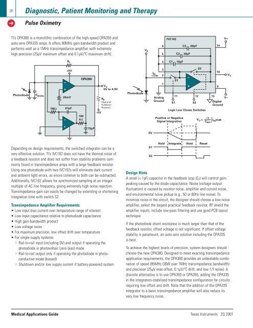
28➔Diagnostic, Patient Monitoring and TherapyPulse OximetryTI’s OPA380 is a monolithic combination of the high-speed OPA355 andauto-zero OPA335 amps. It offers 90MHz gain bandwidth product andperforms well as a 1MHz transimpedance amplifier with extremelyhigh precision (25µV maximum offset and 0.1µV/ºC maximum drift).6V B15IVC102C2C330pF60pF14V+R F+5VOPA380Photodiode C DIODE–20mVR+P1MΩ 67pF–5V100kΩV O0V to 4.9V(OptionalPulldownResistor)PhotodiodeI IN32AnalogGroundS1S111 12 13S2S2Logic Low Closes SwitchesPositive or NegativeSignal Integration∫–1V O =C INT109DigitalGroundI IN (t) dtV–V O4C110pF75pF0VDepending on design requirements, the switched integrator can be avery effective solution. TI’s IVC102 does not have the thermal noise ofa feedback resistor and does not suffer from stability problems commonlyfound in transimpedance amps with a large feedback resistor.Using one photodiode with two IVC102s will eliminate dark currentand ambient light errors, as errors common to both can be subtracted.Additionally, IVC102 allows for synchronized sampling at an integermultiple of AC line frequency, giving extremely high noise rejection.Transimpedance gain can easily be changed by extending or shorteningintegration time with switch S2.Transimpedance Amplifier Requirements• Low input bias current over temperature range of interest• Low input capacitance relative to photodiode capacitance• High gain bandwidth product• Low voltage noise• For maximum precision, low offset drift over temperature• For single-supply systems:• Rail-to-rail input (including 0V) and output if operating thephotodiode in photovoltaic (zero bias) mode• Rail-to-rail output only if operating the photodiode in photoconductivemode (biased)• Shutdown and/or low supply current if battery-powered systemS1S2Hold Integrate Hold ResetDesign HintsA small (< 1pF) capacitor in the feedback loop (C F ) will control gainpeakingcaused by the diode capacitance. Noise (voltage-outputfluctuation) is caused by resistor noise, amplifier and current noise,and environmental noise pickup (e.g., 50 or 60Hz line noise). Tominimize noise in the circuit, the designer should choose a low-noiseamplifier, select the largest practical feedback resistor, RF shield theamplifier inputs, include low-pass filtering and use good PCB layouttechnique.If the photodiode shunt resistance is much larger than that of thefeedback resistor, offset voltage is not significant. If offset voltagestability is paramount, an auto-zero solution including the OPA335is best.To achieve the highest levels of precision, system designers shouldchoose the new OPA380. Designed to meet exacting transimpedanceapplication requirements, the OPA380 provides an unbeatable combinationof speed (85MHz GBW over 1MHz transimpedance bandwidth)and precision (25µV max offset, 0.1µV/ºC drift, and low 1/f noise). Adiscrete alternative is to use OPA350 or OPA355, adding the OPA335in the integrators-stabilized transimpedance configuration for circuitsrequiring low offset and drift. Note that the addition of the OPA335integrator to a basic transimpedance amplifier will also reduce itsvery low frequency noise.<strong>Medical</strong> <strong>Applications</strong> <strong>Guide</strong> Texas Instruments 2Q 2007