PIC18F to PIC24F Migration: An Overview - Microchip
PIC18F to PIC24F Migration: An Overview - Microchip
PIC18F to PIC24F Migration: An Overview - Microchip
Create successful ePaper yourself
Turn your PDF publications into a flip-book with our unique Google optimized e-Paper software.
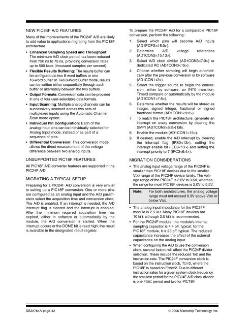
NEW <strong>PIC24F</strong> A/D FEATURESMany of the improvements of the <strong>PIC24F</strong> A/D are likely<strong>to</strong> add value <strong>to</strong> applications migrating from the <strong>PIC18F</strong>architecture.• Enhanced Sampling Speed and Throughput:The minimum A/D clock period has been reducedfrom 750 ns <strong>to</strong> 75 ns, providing conversion ratesup <strong>to</strong> 500 ksps (thousand samples per second).• Flexible Results Buffering: The results buffer canbe configured as two 8-word buffers or one16-word buffer. In Two 8-Word Buffer mode, resultscan be written either sequentially through eachbuffer or alternately between the two buffers.• Output Formats: Conversion data can be providedin one of four user-selectable data formats.• Input Scanning: Multiple analog channels can besuccessively scanned across two sets ofmultiplexed inputs using the Au<strong>to</strong>matic ChannelScan mode option.• Individual Pin Configuration: Each of theanalog input pins can be individually selected for<strong>An</strong>alog Input mode, instead of as part of asequence of pins.• Differential Conversion: This conversion modeallows the direct measurement of the voltagedifference between two analog inputs.UNSUPPORTED <strong>PIC18F</strong> FEATURESAll <strong>PIC18F</strong> A/D converter features are supported in the<strong>PIC24F</strong> A/D.MIGRATING A TYPICAL SETUPPreparing for a <strong>PIC24F</strong> A/D conversion is very similar<strong>to</strong> setting up a <strong>PIC18F</strong> conversion. One or more pinsare configured as an analog input and the A/D parametersselect the acquisition time and conversion clock.The A/D is enabled. If an interrupt is needed, the A/Dinterrupt flag is cleared and the interrupt is enabled.After the minimum required acquisition time hasexpired, either in software or au<strong>to</strong>matically by themodule, the A/D conversion is started. When theinterrupt occurs or the DONE bit is read high, the resultis available in the designated result register.To prepare the <strong>PIC24F</strong> A/D for a comparable <strong>PIC18F</strong>conversion, perform the following:1. Select which pins will become A/D inputs(AD1PCFG).2. Determine A/D voltage references(AD1CON2).3. Select A/D clock divider (AD1CON3) ordedicated RC (AD1CON3).4. Choose whether sampling will begin au<strong>to</strong>maticallyafter the previous conversion or by software(AD1CON1).5. Select the trigger source <strong>to</strong> begin the conversion,either by software, an INT0 transition,Timer3 compare or au<strong>to</strong>matically by the module(AD1CON1).6. Determine whether the results will be s<strong>to</strong>red asinteger, signed integer, fractional or signedfractional format (AD1CON1).7. To match the <strong>PIC18F</strong> architecture, generate aninterrupt on every conversion by clearing theSMPI (AD1CON2) bits.8. Enable the module (AD1CON1).9. If desired, enable the A/D interrupt by clearingthe interrupt flag (IFS0), setting theinterrupt enable bit (IEC0) and setting theinterrupt priority <strong>to</strong> 7 (IPC3).MIGRATION CONSIDERATIONS• The analog input voltage range of the <strong>PIC24F</strong> issmaller than <strong>PIC18F</strong> devices due <strong>to</strong> the smallerVDD range of the <strong>PIC24F</strong> device family. The voltagerange of the <strong>PIC24F</strong> is 2.0V <strong>to</strong> 3.6V, whereasthe range for most <strong>PIC18F</strong> devices is 2.0V <strong>to</strong> 5.5V.Note:For both architectures, the analog voltagerange must not exceed 0.3V above VDD orbelow VSS.• The analog input impedance for the <strong>PIC24F</strong>module is 2.5 kΩ. Many <strong>PIC18F</strong> devices are10 kΩ, although 2.5 kΩ is recommended.• For the <strong>PIC24F</strong> module, the module’s internalsampling capaci<strong>to</strong>r is 4.4 pF, typical; for the<strong>PIC18F</strong> module, it is 25 pF, typical. The reducedcapacitance increases the affect of the externalcapacitance on the analog input.• When configuring the A/D <strong>to</strong> use the conversionclock, several fac<strong>to</strong>rs will affect the <strong>PIC24F</strong> dividerselection. These include the reduced TAD and theinstruction rate. The <strong>PIC24F</strong> conversion clock isbased on the instruction clock, TCY/2, where the<strong>PIC18F</strong> is based on FOSC/2. Due <strong>to</strong> differentinstruction rates for a given system clock frequency,the smallest period for the <strong>PIC24F</strong> A/D clock divideris one FOSC period and two for <strong>PIC18F</strong>.DS39764A-page 42© 2006 <strong>Microchip</strong> Technology Inc.


