System Architecture Design
System Architecture Design
System Architecture Design
You also want an ePaper? Increase the reach of your titles
YUMPU automatically turns print PDFs into web optimized ePapers that Google loves.
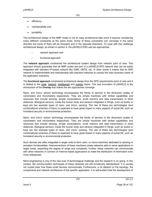
pSHIELD<strong>System</strong> <strong>Architecture</strong> <strong>Design</strong>PU• efficiency,• maintainability and• portability.The architectural design of the NMP nodes is not an easy architectural task since it requires consideringmany different constraints at the same times. Some of these constraints can converge in the samedirection but some of them will be divergent and in the opposite directions. To cope with this challengearchitectural design, as shown in section 4, the pSHIELD ESD use two approaches:- network approach and- functional approach.The network approach constrained the architectural system design from network point of view. Thisapproach should guarantee that all NMP nodes are part of a pSHIELD-SPD network that can be easilyintegrated with standard IP-based network like GSM, UMTS, etc. In other words it means that an SPDnetwork is implementable and interoperable with standard networks to comply the main business cases ofthe application scenarios.The functional approach constrained architectural design from the SPD requirements point of view and itis related to the node, network, middleware and overlay layers. The real innovation of pSHIELD is theintroduction of the Overlay that makes the two approaches converge.Nano- and micro- sensor technology encompasses the family of devices in the dimension scales ofnanometers and micrometers respectively. They are simple machines with limited capabilities andresources that include sensing, simple computations, small memory and data transmission in shortdistances. Biological sensors, inside the human body and sensors integrated in things, such as books orkeys are two example types of nano- and micro- sensing. The rise of these two technologies (andcombinational schemes of them) is expected to have great impact in many aspects of social life, such ashomeland security or environmental protection.Nano- and micro- sensor technology encompasses the family of devices in the dimension scales ofnanometers and micrometers respectively. They are simple machines with limited capabilities andresources that include sensing, simple computations, small memory and data transmission in shortdistances. Biological sensors, inside the human body and sensors integrated in things, such as books orkeys are two example types of nano- and micro- sensing. The rise of these two technologies (andcombinational schemes of them) is expected to have great impact in many aspects of social life, such ashomeland security or environmental protection.Such devices are often integrated in larger units to form nano- or micro-machines dedicated to sensing oractuation functionalities. Interconnections of these machines create networks able to serve applications inlarger areas, expanding the degree of range and complexity. Further, these networks can communicatewith other networks or connect on Internet based applications to make the distribution of information evenmore widespread.Nano-engineering is one of the new eras of technological challenge and the research is on going. In thiscontext, the communication techniques of these networks are still immaturely standardized. It is usuallynot crystal clear how these small devices communicate. Furthermore, a lot depend on the topology, thecomponents and network architecture of the specific application. It is self-evident that the development ofPUD2.3.2Issue 5 Page 29 of 122


