

Deliverables and Services - IHP Microelectronics
Deliverables and Services - IHP Microelectronics
Deliverables and Services - IHP Microelectronics

You also want an ePaper? Increase the reach of your titles
YUMPU automatically turns print PDFs into web optimized ePapers that Google loves.
A u S G e w ä H L t e p r o J e K t e – S e L e C t e d p r o J e C t S<br />
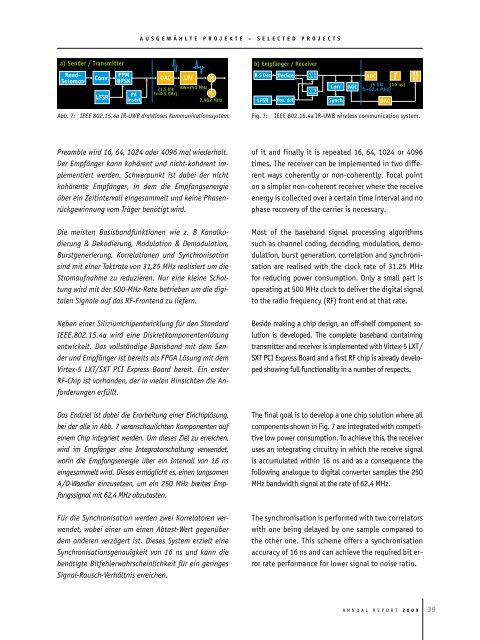
Abb. 7: IEEE 802.15.4a IR-UWB drahtloses Kommunikationssystem. Fig. 7: Ieee 802.15.4a IR-uWB wireless communication system.<br />
Preamble wird 16, 64, 1024 oder 4096 mal wiederholt.<br />
Der Empfänger kann kohärent und nicht-kohärent implementiert<br />
werden. Schwerpunkt ist dabei der nicht<br />
kohärente Empfänger, in dem die Empfangsenergie<br />
über ein Zeitintervall eingesammelt und keine Phasenrückgewinnung<br />
vom Träger benötigt wird.<br />
Die meisten Basisb<strong>and</strong>funktionen wie z. B Kanalkodierung<br />
& Dekodierung, Modulation & Demodulation,<br />
Burstgenerierung, Korrelationen und Synchronisation<br />
sind mit einer Taktrate von 31,25 MHz realisiert um die<br />
Stromaufnahme zu reduzieren. Nur eine kleine Schaltung<br />
wird mit der 500-MHz-Rate betrieben um die digitalen<br />
Signale auf das RF-Frontend zu liefern.<br />
Neben einer Siliziumchipentwicklung für den St<strong>and</strong>ard<br />
IEEE.802.15.4a wird eine Diskretkomponentenlösung<br />
entwickelt. Das vollständige Basisb<strong>and</strong> mit dem Sender<br />
und Empfänger ist bereits als FPGA Lösung mit dem<br />
Virtex-5 LXT/SXT PCI Express Board bereit. Ein erster<br />
RF-Chip ist vorh<strong>and</strong>en, der in vielen Hinsichten die Anforderungen<br />
erfüllt.<br />
Das Endziel ist dabei die Erarbeitung einer Einchiplösung,<br />
bei der alle in Abb. 7 veranschaulichten Komponenten auf<br />
einem Chip integriert werden. Um dieses Ziel zu erreichen,<br />
wird im Empfänger eine Integratorschaltung verwendet,<br />
worin die Empfangsenergie über ein Intervall von 16 ns<br />
eingesammelt wird. Dieses ermöglicht es, einen langsamen<br />
A /D-W<strong>and</strong>ler einzusetzen, um ein 250 MHz breites Empfangssignal<br />
mit 62,4 MHz abzutasten.<br />
Für die Synchronisation werden zwei Korrelatoren verwendet,<br />
wobei einer um einen Abtast-Wert gegenüber<br />
dem <strong>and</strong>eren verzögert ist. Dieses System erzielt eine<br />
Synchronisationsgenauigkeit von 16 ns und kann die<br />
benötigte Bitfehlerwahrscheinlichkeit für ein geringes<br />
Signal-Rausch-Verhältnis erreichen.<br />
of it <strong>and</strong> finally it is repeated 16, 64, 1024 or 4096<br />
times. the receiver can be implemented in two different<br />
ways coherently or non-coherently. Focal point<br />
on a simpler non-coherent receiver where the receive<br />
energy is collected over a certain time interval <strong>and</strong> no<br />
phase recovery of the carrier is necessary.<br />
Most of the baseb<strong>and</strong> signal processing algorithms<br />
such as channel coding, decoding, modulation, demodulation,<br />
burst generation, correlation <strong>and</strong> synchronisation<br />
are realised with the clock rate of 31.25 MHz<br />
for reducing power consumption. only a small part is<br />
operating at 500 MHz clock to deliver the digital signal<br />
to the radio frequency (RF) front end at that rate.<br />
Beside making a chip design, an off-shelf component solution<br />
is developed. the complete baseb<strong>and</strong> containing<br />
transmitter <strong>and</strong> receiver is implemented with Virtex-5 lXt /<br />
SXt pCI express Board <strong>and</strong> a first RF chip is already developed<br />
showing full functionality in a number of respects.<br />
the final goal is to develop a one chip solution where all<br />
components shown in Fig. 7 are integrated with competitive<br />
low power consumption. to achieve this, the receiver<br />
uses an integrating circuitry in which the receive signal<br />
is accumulated within 16 ns <strong>and</strong> as a consequence the<br />
following analogue to digital converter samples the 250<br />
MHz b<strong>and</strong>width signal at the rate of 62.4 MHz.<br />
the synchronisation is performed with two correlators<br />
with one being delayed by one sample compared to<br />
the other one. this scheme offers a synchronisation<br />
accuracy of 16 ns <strong>and</strong> can achieve the required bit error<br />
rate performance for lower signal to noise ratio.<br />
A n n u A l R e p o R t 2 0 0 9<br />
9


