

Deliverables and Services - IHP Microelectronics
Deliverables and Services - IHP Microelectronics
Deliverables and Services - IHP Microelectronics

You also want an ePaper? Increase the reach of your titles
YUMPU automatically turns print PDFs into web optimized ePapers that Google loves.
A u S G e w ä H L t e p r o J e K t e – S e L e C t e d p r o J e C t S<br />
Trotz der erheblichen bisherigen Forschung zu diesen<br />
Materialien stellt die Integration alternativer nichtflüchtiger<br />
Speicher in der Silizium-Mikroelektronik<br />
unter BEOL-Bedingungen wegen zahlreicher R<strong>and</strong>bedingungen<br />
eine Herausforderung dar, z.B. aufgrund<br />
des limitierten thermischen Budgets. Andererseits erweist<br />
sich die Integration von RRAM als vergleichsweise<br />
einfach, kosteneffektiv und BEOL-kompatibel. Darüber<br />
hinaus bietet RRAM die Vorteile einer hohen Retention<br />
und einer reduzierten Leistungsaufnahme.<br />
Denkbare Mechanismen für das resistive Schalten in<br />
MIM-Systemen bestehen häufig aus einer Kombination<br />
physikalischer und/oder chemischer Effekte. Jüngste<br />
Studien haben gezeigt, dass die elektrochemische Migration<br />
von Sauerstoff-Ionen den resistiven Schalteffekt<br />
auslöst.<br />
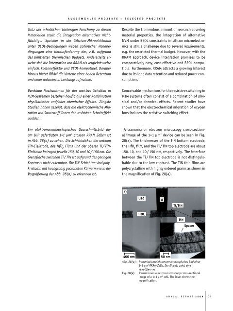
Ein elektronenmikroskopisches Querschnittsbild der<br />
am <strong>IHP</strong> gefertigten 1×1 µm 2 grossen RRAM Zellen ist<br />
in Abb. 28(a) zu sehen. Die Schichtdicken der unteren<br />
TiN-Elektrode, des HfO 2 Films und der oberen Ti / TiN-<br />
Elektrode betragen jeweils 150, 10 und 10 / 150 nm. Die<br />
Grenzfläche zwischen Ti / TiN ist aufgrund des geringen<br />
Kontrasts nicht erkennbar. Die TiN-Schichten sind polykristallin<br />
mit hochgradig geordneten Körnern wie in der<br />
Vergrößerung der Abb. 28(a) zu erkennen ist.<br />
Despite the tremendous amount of research covering<br />
material properties, the integration of alternative<br />
nVM under Beol constraints in silicon microelectronics<br />
is still a challenge due to several requirements,<br />
e.g. the restricted thermal budget. However, with the<br />
RRAM approach, device integration promises to be<br />
comparatively easy, cost-effective <strong>and</strong> Beol compatible.<br />
Furthermore, RRAM attracts a growing interest<br />
due to its long data retention <strong>and</strong> reduced power consumption.<br />
Conceivable mechanisms for the resistive switching in<br />
MIM systems often consist of a combination of physical<br />
<strong>and</strong> /or chemical effects. Recent studies have<br />
shown that the electrochemical migration of oxygen<br />
ions induces the resistive switching effect.<br />
A transmission electron microscopy cross-sectional<br />
image of the 1×1 µm 2 device can be seen in Fig.<br />
28(a). the thicknesses of the tin bottom electrode,<br />
the Hfo 2 film, <strong>and</strong> the ti / tin top electrode are about<br />
150, 10, <strong>and</strong> 10 / 150 nm, respectively. the interface<br />
between the ti / tin top electrode is not distinguishable<br />
due to the low contrast. the tin thin films are<br />
polycrystalline with highly ordered grains as shown in<br />
the magnification of Fig. 28(a).<br />
Abb. 28(a): Transmissionselektronenmikroskopisches Bild einer<br />
1×1 µm 2 RRAM-Zelle. Der Einsatz zeigt eine<br />
Vergrößerung.<br />
Fig. 28(a): transmission electron microscopy cross-sectional<br />
image of a 1×1 µm 2 cell. the inset shows the<br />
magnification.<br />
A n n u A l R e p o R t 2 0 0 9<br />
7


