

Deliverables and Services - IHP Microelectronics
Deliverables and Services - IHP Microelectronics
Deliverables and Services - IHP Microelectronics

Create successful ePaper yourself
Turn your PDF publications into a flip-book with our unique Google optimized e-Paper software.
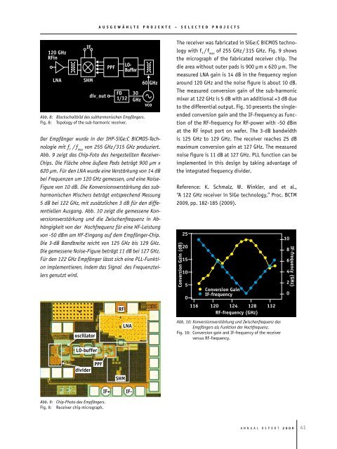
Abb. 8: Blockschaltbild des subharmonischen Empfängers.<br />
Fig. 8: topology of the sub-harmonic receiver.<br />
A u S G e w ä H L t e p r o J e K t e – S e L e C t e d p r o J e C t S<br />
Der Empfänger wurde in der <strong>IHP</strong>-SiGe:C BiCMOS-Technologie<br />
mit f T / f max von 255 GHz /315 GHz produziert.<br />
Abb. 9 zeigt das Chip-Foto des hergestellten Receiver-<br />
Chips. Die Fläche ohne äußere Pads beträgt 900 µm x<br />
620 µm. Für den LNA wurde eine Verstärkung von 14 dB<br />
bei Frequenzen um 120 GHz gemessen, und eine Noise-<br />
Figure von 10 dB. Die Konversionsverstärkung des subharmonischen<br />
Mischers beträgt entsprechend Messung<br />
5 dB bei 122 GHz, mit zusätzlichen 3 dB für den differentiellen<br />
Ausgang. Abb. 10 zeigt die gemessene Konversionsverstärkung<br />
und die Zwischenfrequenz in Abhängigkeit<br />
von der Hochfrequenz für eine HF-Leistung<br />
von -50 dBm am HF-Eingang auf dem Empfänger-Chip.<br />
Die 3-dB B<strong>and</strong>breite reicht von 125 GHz bis 129 GHz.<br />
Die gemessene Noise-Figure beträgt 11 dB bei 127 GHz.<br />
Für den 122 GHz Empfänger lässt sich eine PLL-Funktion<br />
implementieren, indem das Signal des Frequenzteilers<br />
genutzt wird.<br />
Abb. 9: Chip-Photo des Empfängers.<br />
Fig. 9: Receiver chip micrograph.<br />
the receiver was fabricated in SiGe:C BiCMoS technology<br />
with f t / f max of 255 GHz / 315 GHz. Fig. 9 shows<br />
the micrograph of the fabricated receiver chip. the<br />
die area without outer pads is 900 µm x 620 µm. the<br />
measured lnA gain is 14 dB in the frequency region<br />
around 120 GHz <strong>and</strong> the noise figure is about 10 dB.<br />
the measured conversion gain of the sub-harmonic<br />
mixer at 122 GHz is 5 dB with an additional +3 dB due<br />
to the differential output. Fig. 10 presents the singleended<br />
conversion gain <strong>and</strong> the IF-frequency as function<br />
of the RF-frequency for RF-power with -50 dBm<br />
at the RF input port on wafer. the 3-dB b<strong>and</strong>width<br />
is 125 GHz to 129 GHz. the receiver reaches 25 dB<br />
maximum conversion gain at 127 GHz. the measured<br />
noise figure is 11 dB at 127 GHz. pll function can be<br />
implemented in this design by taking advantage of<br />
the integrated frequency divider.<br />
Reference: K. Schmalz, W. Winkler, <strong>and</strong> et al.,<br />
“A 122 GHz receiver in SiGe technology,” proc. BCtM<br />
2009, pp. 182-185 (2009).<br />
Abb. 10: Konversionsverstärkung und Zwischenfrequenz des<br />
Empfängers als Funktion der Hochfrequenz.<br />
Fig. 10: Conversion gain <strong>and</strong> IF-frequency of the receiver<br />
versus RF-frequency.<br />
A n n u A l R e p o R t 2 0 0 9


