

Deliverables and Services - IHP Microelectronics
Deliverables and Services - IHP Microelectronics
Deliverables and Services - IHP Microelectronics

You also want an ePaper? Increase the reach of your titles
YUMPU automatically turns print PDFs into web optimized ePapers that Google loves.
A u S G e w ä H L t e p r o J e K t e – S e L e C t e d p r o J e C t S<br />
Alle Strukturen, die der Temperung bei 400 °C nicht<br />
unterzogen wurden, wiesen eine größere Effizienz für<br />
den strahlenden Übergang auf, als die beh<strong>and</strong>elten<br />
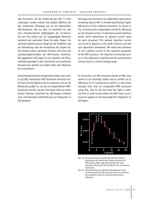
MIS-Strukturen. Wie aus Abb. 34 ersichtlich ist, tritt<br />
eine charakteristische Abhängigkeit der EL-Intensität<br />
vom Fluss-Strom auf. Ein ausgeprägtes Maximum<br />
bestimmt den optimalen Strom für jeden Stapel. Der<br />
optimale Injektionsstrom hängt von der Oxiddicke und<br />
der Beh<strong>and</strong>lung nach der Herstellung des Stapels ab.<br />
Die Existenz dieses optimalen Stromes wird durch die<br />
Injektionseigenschaften der MIS-Struktur bestimmt.<br />
Bei gegebenem MIS-Stapel ist die Injektion der Minoritätsladungsträger<br />
in das Substrat für eine bestimmte<br />
Vorspannung optimal und liefert dann das Maximum<br />
der Lumineszenz.<br />
Zusammenfassend kann festgestellt werden, dass unsere<br />
auf HfO 2 basierenden MIS-Strukturen thermisch stabil<br />
sind und eine Effizienz der EL aufweisen, die um ein<br />
Mehrfaches größer ist, als die von vergleichbaren MOS-<br />
Strukturen mit SiO 2 . Da das Licht dieser LEDs aus einem<br />
kleinen Volumen unterhalb des MIS-Stapels emittiert<br />
wird, sind derartige Lichtemitter gut zur Integration in<br />
SOI geeignet.<br />
Generally, the structures not subjected to passivation<br />
annealing step at 400 °C showed significantly higher<br />
efficiencies of the radiative transition. As shown in<br />
Fig. 34 there exists a dependence of the el efficiency<br />
on the forward current. A well pronounced maximum<br />
exists, which determines an optimal current value<br />
for each structure. this optimal injection current<br />
was found to depend on the oxide thickness <strong>and</strong> the<br />
post deposition treatments. We relate the existence<br />
of such optimal current to the injection properties<br />
of the MIS structure. the injection of minority carriers<br />
in the substrate is optimal <strong>and</strong> the luminescence<br />
strong only for a certain voltage range.<br />
In conclusion, our MIS structures based on Hfo 2 were<br />
shown to be thermally stable <strong>and</strong> to exhibit an el<br />
efficiency for Si luminescence which is a few times<br />
stronger than that for comparable MoS structures<br />
using Sio 2 . Due to the fact that the light is emitted<br />
from a small volume below the MIS stack, such a<br />
structure appears to be favourable for integration in<br />
SoI layers.<br />
Abb. 34: Die auf den Strom normierte Intensität der Elektrolumineszenz<br />
als Funktion des Stromes, der durch die<br />
MIS-Struktur fließt, zeigt das Vorh<strong>and</strong>ensein eines<br />
optimalen Stromes, für den die Effizienz der Lumineszenz<br />
maximal ist.<br />
Fig. 34: electroluminescence efficiency dependence on the<br />
current through the MIS structure shows the existence<br />
of an optimal current for maximal luminescence<br />
efficiency.<br />
A n n u A l R e p o R t 2 0 0 9<br />
6


