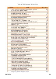
DATA SHEET - IEETA
DATA SHEET - IEETA
DATA SHEET - IEETA

Create successful ePaper yourself
Turn your PDF publications into a flip-book with our unique Google optimized e-Paper software.
Philips Semiconductors Product specification<br />
8-bit microcontroller with on-chip CAN P8xC592<br />
11 TIMERS/COUNTERS<br />
The P8xC592 contains:<br />
• Three 16-bit timer/event counters:<br />
Timer 0, Timer 1 and Timer T2<br />
• One 8-bit timer, T3 (Watchdog WDT).<br />
11.1 Timer 0 and Timer 1<br />
Timer 0 and Timer 1 may be programmed to carry out the<br />
following functions:<br />
• Measure time intervals and pulse durations<br />
• Count events<br />
• Generate interrupt requests.<br />
Timer 0 and Timer 1 can be programmed independently to<br />
operate in 3 modes:<br />
Mode 0 8-bit timer or 8-bit counter each with divide-by-32<br />
prescaler.<br />
Mode 1 16-bit timer-interval or event counter.<br />
Mode 2 8-bit timer-interval or event counter with<br />
automatic reload upon overflow.<br />
Timer 0 can be programmed to operate in an additional<br />
mode as follows:<br />
Mode 3 one 8-bit time-interval or event counter and one<br />
8-bit timer-interval counter.<br />
When Timer 0 is in Mode 3, Timer 1 can be programmed<br />
to operate in Modes 0, 1 or 2 but cannot set an interrupt<br />
flag or generate an interrupt. However, the overflow from<br />
Timer 1 can be used to pulse the Serial Port baud-rate<br />
generator.<br />
The frequency handling range of these counters with a<br />
16 MHz crystal is as follows:<br />
• In the timer function, the timer is incremented at a<br />
frequency of 1.33 MHz ( 1 ⁄12 of the oscillator frequency)<br />
• 0 Hz to an upper limit of 0.66 MHz ( 1 ⁄24 of the oscillator<br />
frequency) when programmed for external inputs.<br />
Both internal and external inputs can be gated to the<br />
counter by a second external source for directly measuring<br />
pulse durations. When configured as a counter, the<br />
register is incremented on every falling edge on the<br />
corresponding input pin, T0 or T1.<br />
The earliest moment, when the incremented register value<br />
can be read is during the second machine cycle following<br />
the machine cycle within which the incrementing pulse<br />
occurred.The counters are started and stopped under<br />
software control. Each one sets its interrupt request flag<br />
1996 Jun 27 21<br />
when it overflows from all HIGHs to all LOWs<br />
(or automatic reload value), with the exception of Mode 3<br />
as previously described.<br />
11.2 Timer T2 Capture and Compare Logic<br />
Timer T2 is a 16-bit timer/counter which has capture and<br />
compare facilities (see Fig.11).<br />
The 16-bit timer/counter is clocked via a prescaler with a<br />
programmable division factor of 1, 2, 4 or 8. The input of<br />
the prescaler is clocked with 1 ⁄12 of the oscillator<br />
frequency, or by an external source connected to the T2<br />
input, or it is switched off. The maximum repetition rate of<br />
the external clock source is 1 ⁄12fCLK, twice that of Timer 0<br />
and Timer 1. The prescaler is incremented on a rising<br />
edge. It is cleared if its division factor or its input source is<br />
changed, or if the timer/counter is reset.<br />
T2 is readable ‘on the fly’, without any extra read latches;<br />
this means that software precautions have to be taken<br />
against misinterpretation at overflow from least to most<br />
significant byte while T2 is being read. T2 is not loadable<br />
and is reset by the RST signal or at the positive edge of the<br />
input signal RT2, if enabled. In the Idle mode the<br />
timer/counter and prescaler are reset and halted.<br />
T2 is connected to four 16-bit Capture Registers: CT0,<br />
CT1, CT2 and CT3. A rising or falling edge on the inputs<br />
CT0I, CT1I, CT2I or CT3I (alternative function of Port 1)<br />
results in loading the contents of T2 into the respective<br />
Capture Registers and an interrupt request.<br />
Using the Capture Register CTCON, these inputs may<br />
invoke capture and interrupt request on a positive edge, a<br />
negative edge or on both edges. If neither a positive nor a<br />
negative edge is selected for capture input, no capture or<br />
interrupt request can be generated by this input.<br />
The contents of the Compare Registers CM0, CM1 and<br />
CM2 are continually compared with the counter value of<br />
Timer T2. When a match occurs, an interrupt may be<br />
invoked. A match of CM0 sets the bits 0 to 5 of Port 4, a<br />
CM1 match resets these bits and a CM2 match toggles bits<br />
6 and 7 of Port 4, provided these functions are enabled by<br />
the STE/RTE registers. A match of CM0 and CM1 at the<br />
same time results in resetting bits 0 to 5 of Port 4. CM0,<br />
CM1 and CM2 are reset by the RST signal.<br />
Port 4 can be read and written by software without<br />
affecting the toggle, set and reset signals. At a byte<br />
overflow of the least significant byte, or at a 16-bit overflow<br />
of the timer/counter, an interrupt sharing the same<br />
interrupt vector is requested. Either one or both of these<br />
overflows can be programmed to request an interrupt.<br />
All interrupt flags must be reset by software.