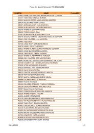
DATA SHEET - IEETA
DATA SHEET - IEETA
DATA SHEET - IEETA

Create successful ePaper yourself
Turn your PDF publications into a flip-book with our unique Google optimized e-Paper software.
Philips Semiconductors Product specification<br />
8-bit microcontroller with on-chip CAN P8xC592<br />
13.5.10 BUS TIMING REGISTER 1(BTR1)<br />
The contents of Bus Timing Register 1 defines the length<br />
of the bit period, the location of the sample point and the<br />
number of samples to be taken at each sample point.<br />
Table 47 Bus Timing Register 1 (address 7)<br />
Table 48 Description of the BTR1 bits<br />
1996 Jun 27 43<br />
This register can be accessed (read/write) if the Reset<br />
Request bit is set HIGH (present).For further information<br />
on bus timing, see Sections 13.5.9 and 13.5.18.<br />
7 6 5 4 3 2 1 0<br />
SAM TSEG2.2 TSEG2.1 TSEG2.0 TSEG1.3 TSEG1.2 TSEG1.1 TSEG1.0<br />
BIT SYMBOL FUNCTION<br />
7 SAM Sampling. If the bit SAM is:<br />
HIGH (3 samples), then three samples are taken. This is recommended for slow/medium speed<br />
buses (SAE class A and B) where filtering of spikes on the bus-line is beneficial<br />
(see Section 13.5.19.6)<br />
LOW (1 sample), the bus is sampled once.<br />
This is recommended for high speed buses (SAE class C).<br />
6 TSEG2.2 Time Segment 1 (TSEG1) and Time Segment 2 (TSEG2).<br />
5 TSEG2.1 TSEG1 determines the number of clock cycles per bit period and the location of the sample point<br />
4 TSEG2.0 tTSEG1 = tSCL ( 8TSEG1.3 + 4TSEG1.2 + 2TSEG1.1 + TSEG1.0 + 1)<br />
.<br />
3 TSEG1.3<br />
TSEG2 determines the number of clock cycles per bit period and the location of the sample point:<br />
2<br />
1<br />
TSEG1.2<br />
TSEG1.1<br />
tTSEG2 =<br />
tSCL ( 4TSEG2.2 + 2TSEG2.1 + TSEG2.0 + 1)<br />
.<br />
0 TSEG1.0